本章主要新建ddr3工程,然后将官方的ddr3仿真文件加入到工程里进行仿真,开发环境2020.1。
新建ddr3_test工程
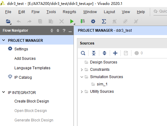
新建ddr3工程顶层
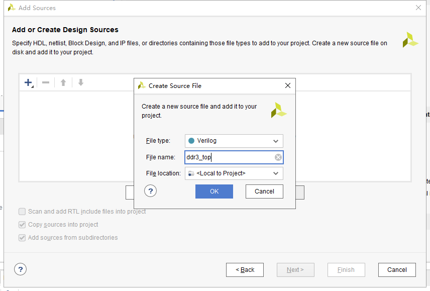
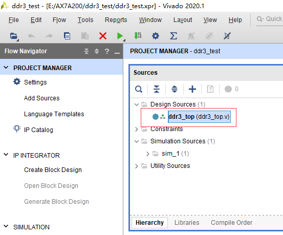
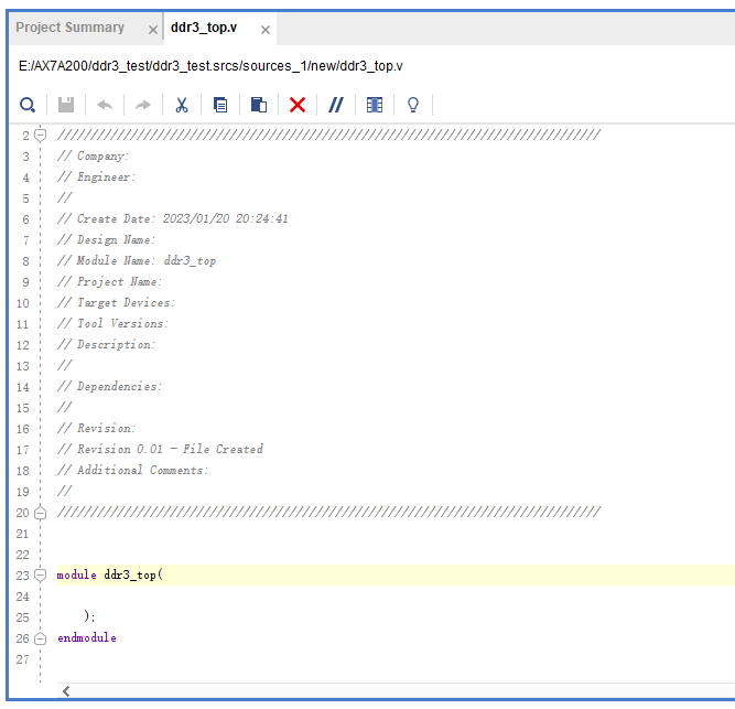
新建的ddr3_top顶层文件,目前还是空白的
调用mig控制器,请参考我上一个章节,这里不在具体写调用过程
AX7A200教程(1):DDR3仿真平台搭建(一)
工程里调用mig控制器,如下图所示

将mig控制器例化到ddr3_top顶层
`timescale 1ns / 1ps
//
// Company:
// Engineer:
//
// Create Date: 2023/01/20 20:24:41
// Design Name:
// Module Name: ddr3_top
// Project Name:
// Target Devices:
// Tool Versions:
// Description:
//
// Dependencies:
//
// Revision:
// Revision 0.01 - File Created
// Additional Comments:
//
//


module ddr3_top(
    //clock
    input               sys_clk_i,//200M
    //reset
    input               sys_rst,
   // Inouts
   inout [31:0]         ddr3_dq,
   inout [3:0]          ddr3_dqs_n,
   inout [3:0]          ddr3_dqs_p,
   // Outputs
   output [14:0]        ddr3_addr,
   output [2:0]         ddr3_ba,
   output               ddr3_ras_n,
   output               ddr3_cas_n,
   output               ddr3_we_n,
   output               ddr3_reset_n,
   output [0:0]         ddr3_ck_p,
   output [0:0]         ddr3_ck_n,
   output [0:0]         ddr3_cke,
   output [0:0]         ddr3_cs_n,
   output [3:0]         ddr3_dm,
   output [0:0]         ddr3_odt

    );

  wire [28:0]                           app_addr;               //DDR3地址
  wire [2:0]                            app_cmd;                //MIG IP核操作命令,读或者写
  wire                                  app_en;                 //MIG IP发送命令使能
  wire                                  app_rdy;                //MIG 命令接收准备好标志
  wire [255:0]                          app_rd_data;            //用户读数据
  wire                                  app_rd_data_end;        //突发读当前时钟最后一个数据
  wire                                  app_rd_data_valid;      //读数据有效
  wire [255:0]                          app_wdf_data;           //用户写数据
  wire                                  app_wdf_end;            //突发写当前时钟最后一个数据
  wire [31:0]                           app_wdf_mask;
  wire                                  app_wdf_rdy;            //MIG数据接收准备好
  wire                                  app_sr_active;
  wire                                  app_ref_ack;
  wire                                  app_zq_ack;
  wire                                  app_wdf_wren;
  wire                                  ui_clk;                //用户时钟
  wire                                  ui_clk_sync_rst;       //复位,高有效

  mig_7series_0 u_mig_7series_0 (


    // Memory interface ports
    .ddr3_addr                      (ddr3_addr),  // output [14:0]        ddr3_addr
    .ddr3_ba                        (ddr3_ba),  // output [2:0]        ddr3_ba
    .ddr3_cas_n                     (ddr3_cas_n),  // output            ddr3_cas_n
    .ddr3_ck_n                      (ddr3_ck_n),  // output [0:0]        ddr3_ck_n
    .ddr3_ck_p                      (ddr3_ck_p),  // output [0:0]        ddr3_ck_p
    .ddr3_cke                       (ddr3_cke),  // output [0:0]        ddr3_cke
    .ddr3_ras_n                     (ddr3_ras_n),  // output            ddr3_ras_n
    .ddr3_reset_n                   (ddr3_reset_n),  // output            ddr3_reset_n
    .ddr3_we_n                      (ddr3_we_n),  // output            ddr3_we_n
    .ddr3_dq                        (ddr3_dq),  // inout [31:0]        ddr3_dq
    .ddr3_dqs_n                     (ddr3_dqs_n),  // inout [3:0]        ddr3_dqs_n
    .ddr3_dqs_p                     (ddr3_dqs_p),  // inout [3:0]        ddr3_dqs_p
    .init_calib_complete            (init_calib_complete),  // output            init_calib_complete


    .ddr3_cs_n                      (ddr3_cs_n),  // output [0:0]        ddr3_cs_n
    .ddr3_dm                        (ddr3_dm),  // output [3:0]        ddr3_dm
    .ddr3_odt                       (ddr3_odt),  // output [0:0]        ddr3_odt
    // Application interface ports
    .app_addr                       (app_addr),  // input [28:0]        app_addr
    .app_cmd                        (app_cmd),  // input [2:0]        app_cmd
    .app_en                         (app_en),  // input                app_en
    .app_wdf_data                   (app_wdf_data),  // input [255:0]        app_wdf_data
    .app_wdf_end                    (app_wdf_end),  // input                app_wdf_end
    .app_wdf_wren                   (app_wdf_wren),  // input                app_wdf_wren
    .app_rd_data                    (app_rd_data),  // output [255:0]        app_rd_data
    .app_rd_data_end                (app_rd_data_end),  // output            app_rd_data_end
    .app_rd_data_valid              (app_rd_data_valid),  // output            app_rd_data_valid
    .app_rdy                        (app_rdy),  // output            app_rdy
    .app_wdf_rdy                    (app_wdf_rdy),  // output            app_wdf_rdy
    .app_sr_req                     (1'b0),  // input            app_sr_req
    .app_ref_req                    (1'b0),  // input            app_ref_req
    .app_zq_req                     (1'b0),  // input            app_zq_req
    .app_sr_active                  (app_sr_active),  // output            app_sr_active
    .app_ref_ack                    (app_ref_ack),  // output            app_ref_ack
    .app_zq_ack                     (app_zq_ack),  // output            app_zq_ack
    .ui_clk                         (ui_clk),  // output            ui_clk
    .ui_clk_sync_rst                (ui_clk_sync_rst),  // output            ui_clk_sync_rst
    .app_wdf_mask                   (32'd0),  // input [31:0]        app_wdf_mask
    // System Clock Ports
    .sys_clk_i                      (sys_clk_i),
    .sys_rst                        (sys_rst) // input sys_rst

    );
endmodule
在这里往后都比较复杂,务必按照步骤来做,目前这种仿真ddr3的方法csdn上没有,但这种方式仿真不容易出错,但搭建起来比较麻烦
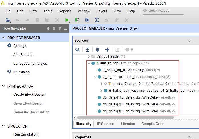
在我上篇博客中提到,xilinx官方提供了mig控制器的仿真脚本,那么现在我们就将上篇博客工程中的仿真文件,导入到这个新建的ddr3工程的仿真目录里面,上篇博客里的仿真文件如下图所示,但我们只需导入部分文件即可
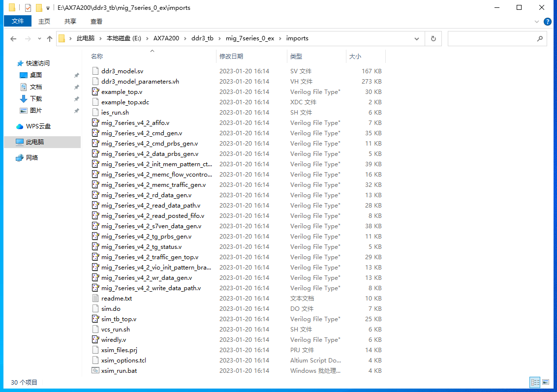
找到xlinx官方的仿真路径下的文件,如下图所示
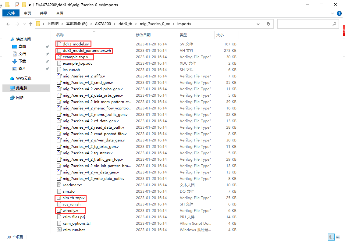
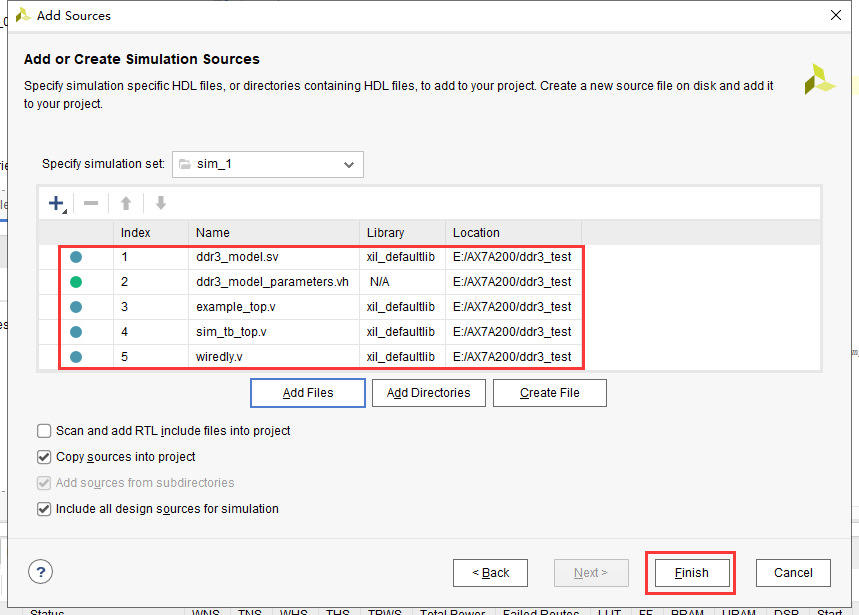
复制我选中的这五个文件,复制到我们现在新建的这个工程下面
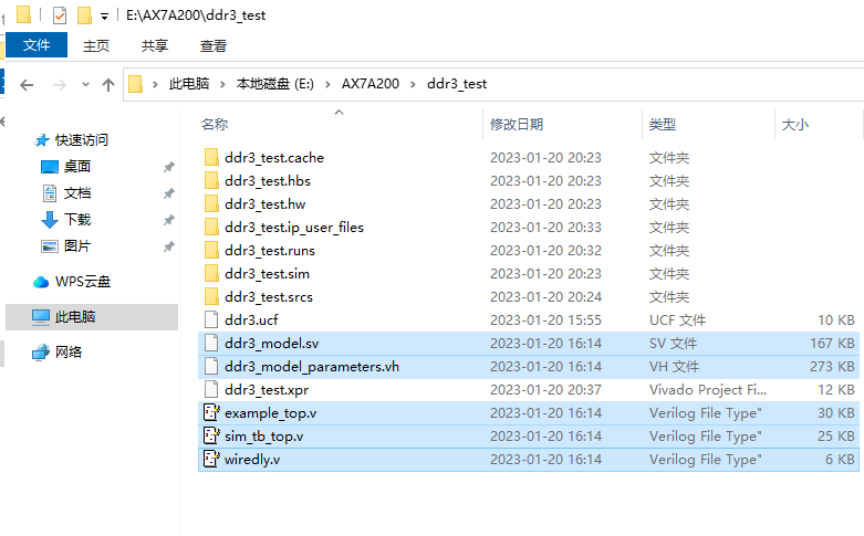
复制到工程文件夹里面
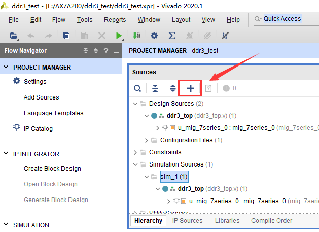
点击“+”加入仿真文件
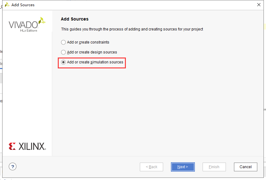
选择加入仿真文件
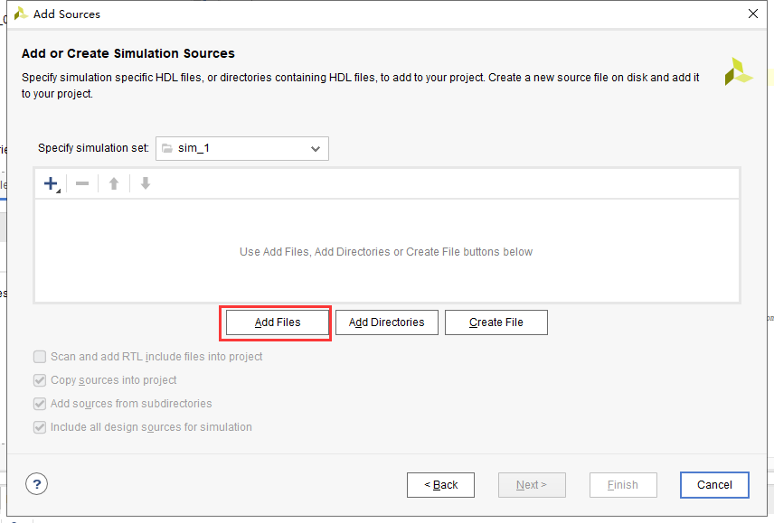
选择Add Files加入文件
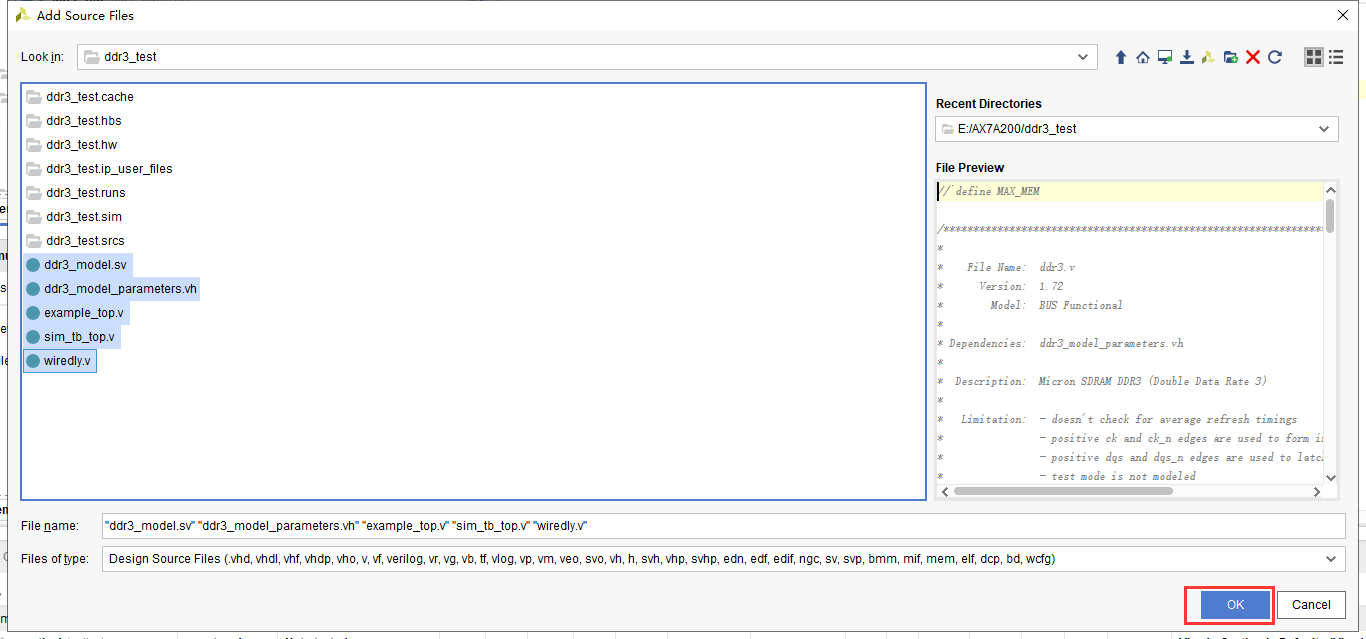
选择这五个文件,点击OK加入进去
点击Finish,加入到仿真目录下
可以看到仿真目录sim也出现了官方提供的仿真文件
修改example_top文件,也就是红框选择的这个文件

修改后的example_top文件
//*****************************************************************************
// (c) Copyright 2009 - 2013 Xilinx, Inc. All rights reserved.
//
// This file contains confidential and proprietary information
// of Xilinx, Inc. and is protected under U.S. and
// international copyright and other intellectual property
// laws.
//
// DISCLAIMER
// This disclaimer is not a license and does not grant any
// rights to the materials distributed herewith. Except as
// otherwise provided in a valid license issued to you by
// Xilinx, and to the maximum extent permitted by applicable
// law: (1) THESE MATERIALS ARE MADE AVAILABLE "AS IS" AND
// WITH ALL FAULTS, AND XILINX HEREBY DISCLAIMS ALL WARRANTIES
// AND CONDITIONS, EXPRESS, IMPLIED, OR STATUTORY, INCLUDING
// BUT NOT LIMITED TO WARRANTIES OF MERCHANTABILITY, NON-
// INFRINGEMENT, OR FITNESS FOR ANY PARTICULAR PURPOSE; and
// (2) Xilinx shall not be liable (whether in contract or tort,
// including negligence, or under any other theory of
// liability) for any loss or damage of any kind or nature
// related to, arising under or in connection with these
// materials, including for any direct, or any indirect,
// special, incidental, or consequential loss or damage
// (including loss of data, profits, goodwill, or any type of
// loss or damage suffered as a result of any action brought
// by a third party) even if such damage or loss was
// reasonably foreseeable or Xilinx had been advised of the
// possibility of the same.
//
// CRITICAL APPLICATIONS
// Xilinx products are not designed or intended to be fail-
// safe, or for use in any application requiring fail-safe
// performance, such as life-support or safety devices or
// systems, Class III medical devices, nuclear facilities,
// applications related to the deployment of airbags, or any
// other applications that could lead to death, personal
// injury, or severe property or environmental damage
// (individually and collectively, "Critical
// Applications"). Customer assumes the sole risk and
// liability of any use of Xilinx products in Critical
// Applications, subject only to applicable laws and
// regulations governing limitations on product liability.
//
// THIS COPYRIGHT NOTICE AND DISCLAIMER MUST BE RETAINED AS
// PART OF THIS FILE AT ALL TIMES.
//
//*****************************************************************************
// ____ ____
// / /\/ /
// /___/ \ / Vendor : Xilinx
// \ \ \/ Version : 4.2
// \ \ Application : MIG
// / / Filename : example_top.v
// /___/ /\ Date Last Modified : $Date: 2011/06/02 08:35:03 $
// \ \ / \ Date Created : Tue Sept 21 2010
// \___\/\___\
//
// Device : 7 Series
// Design Name : DDR3 SDRAM
// Purpose :
// Top-level module. This module serves as an example,
// and allows the user to synthesize a self-contained design,
// which they can be used to test their hardware.
// In addition to the memory controller, the module instantiates:
// 1. Synthesizable testbench - used to model user's backend logic
// and generate different traffic patterns
// Reference :
// Revision History :
//*****************************************************************************
//`define SKIP_CALIB
`timescale 1ps/1ps
module example_top #
(
//***************************************************************************
// Traffic Gen related parameters
//***************************************************************************
parameter PORT_MODE = "BI_MODE",
parameter DATA_MODE = 4'b0010,
parameter TST_MEM_INSTR_MODE = "R_W_INSTR_MODE",
parameter EYE_TEST = "FALSE",
// set EYE_TEST = "TRUE" to probe memory
// signals. Traffic Generator will only
// write to one single location and no
// read transactions will be generated.
parameter DATA_PATTERN = "DGEN_ALL",
// For small devices, choose one only.
// For large device, choose "DGEN_ALL"
// "DGEN_HAMMER", "DGEN_WALKING1",
// "DGEN_WALKING0","DGEN_ADDR","
// "DGEN_NEIGHBOR","DGEN_PRBS","DGEN_ALL"
parameter CMD_PATTERN = "CGEN_ALL",
// "CGEN_PRBS","CGEN_FIXED","CGEN_BRAM",
// "CGEN_SEQUENTIAL", "CGEN_ALL"
parameter CMD_WDT = 'h3FF,
parameter WR_WDT = 'h1FFF,
parameter RD_WDT = 'h3FF,
parameter SEL_VICTIM_LINE = 0,
parameter BEGIN_ADDRESS = 32'h00000000,
parameter END_ADDRESS = 32'h00ffffff,
parameter PRBS_EADDR_MASK_POS = 32'hff000000,
//***************************************************************************
// The following parameters refer to width of various ports
//***************************************************************************
parameter CK_WIDTH = 1,
// # of CK/CK# outputs to memory.
parameter nCS_PER_RANK = 1,
// # of unique CS outputs per rank for phy
parameter CKE_WIDTH = 1,
// # of CKE outputs to memory.
parameter DM_WIDTH = 4,
// # of DM (data mask)
parameter ODT_WIDTH = 1,
// # of ODT outputs to memory.
parameter BANK_WIDTH = 3,
// # of memory Bank Address bits.
parameter COL_WIDTH = 10,
// # of memory Column Address bits.
parameter CS_WIDTH = 1,
// # of unique CS outputs to memory.
parameter DQ_WIDTH = 32,
// # of DQ (data)
parameter DQS_WIDTH = 4,
parameter DQS_CNT_WIDTH = 2,
// = ceil(log2(DQS_WIDTH))
parameter DRAM_WIDTH = 8,
// # of DQ per DQS
parameter ECC = "OFF",
parameter ECC_TEST = "OFF",
//parameter nBANK_MACHS = 4,
parameter nBANK_MACHS = 4,
parameter RANKS = 1,
// # of Ranks.
parameter ROW_WIDTH = 15,
// # of memory Row Address bits.
parameter ADDR_WIDTH = 29,
// # = RANK_WIDTH + BANK_WIDTH
// + ROW_WIDTH + COL_WIDTH;
// Chip Select is always tied to low for
// single rank devices
//***************************************************************************
// The following parameters are mode register settings
//***************************************************************************
parameter BURST_MODE = "8",
// DDR3 SDRAM:
// Burst Length (Mode Register 0).
// # = "8", "4", "OTF".
// DDR2 SDRAM:
// Burst Length (Mode Register).
// # = "8", "4".
//***************************************************************************
// The following parameters are multiplier and divisor factors for PLLE2.
// Based on the selected design frequency these parameters vary.
//***************************************************************************
parameter CLKIN_PERIOD = 5000,
// Input Clock Period
parameter CLKFBOUT_MULT = 4,
// write PLL VCO multiplier
parameter DIVCLK_DIVIDE = 1,
// write PLL VCO divisor
parameter CLKOUT0_PHASE = 0.0,
// Phase for PLL output clock (CLKOUT0)
parameter CLKOUT0_DIVIDE = 1,
// VCO output divisor for PLL output clock (CLKOUT0)
parameter CLKOUT1_DIVIDE = 2,
// VCO output divisor for PLL output clock (CLKOUT1)
parameter CLKOUT2_DIVIDE = 32,
// VCO output divisor for PLL output clock (CLKOUT2)
parameter CLKOUT3_DIVIDE = 8,
// VCO output divisor for PLL output clock (CLKOUT3)
parameter MMCM_VCO = 800,
// Max Freq (MHz) of MMCM VCO
parameter MMCM_MULT_F = 8,
// write MMCM VCO multiplier
parameter MMCM_DIVCLK_DIVIDE = 1,
// write MMCM VCO divisor
//***************************************************************************
// Simulation parameters
//***************************************************************************
parameter SIMULATION = "FALSE",
// Should be TRUE during design simulations and
// FALSE during implementations
//***************************************************************************
// IODELAY and PHY related parameters
//***************************************************************************
parameter TCQ = 100,
parameter DRAM_TYPE = "DDR3",
//***************************************************************************
// System clock frequency parameters
//***************************************************************************
parameter nCK_PER_CLK = 4,
// # of memory CKs per fabric CLK
//***************************************************************************
// Debug parameters
//***************************************************************************
parameter DEBUG_PORT = "OFF",
// # = "ON" Enable debug signals/controls.
// = "OFF" Disable debug signals/controls.
parameter RST_ACT_LOW = 1
// =1 for active low reset,
// =0 for active high.
)
(
// Inouts
inout [31:0] ddr3_dq,
inout [3:0] ddr3_dqs_n,
inout [3:0] ddr3_dqs_p,
// Outputs
output [14:0] ddr3_addr,
output [2:0] ddr3_ba,
output ddr3_ras_n,
output ddr3_cas_n,
output ddr3_we_n,
output ddr3_reset_n,
output [0:0] ddr3_ck_p,
output [0:0] ddr3_ck_n,
output [0:0] ddr3_cke,
output [0:0] ddr3_cs_n,
output [3:0] ddr3_dm,
output [0:0] ddr3_odt,
// Inputs
// Single-ended system clock
input sys_clk_i,
output tg_compare_error,
output init_calib_complete,
// System reset - Default polarity of sys_rst pin is Active Low.
// System reset polarity will change based on the option
// selected in GUI.
input sys_rst
);
function integer clogb2 (input integer size);
begin
size = size - 1;
for (clogb2=1; size>1; clogb2=clogb2+1)
size = size >> 1;
end
endfunction // clogb2
function integer STR_TO_INT;
input [7:0] in;
begin
if(in == "8")
STR_TO_INT = 8;
else if(in == "4")
STR_TO_INT = 4;
else
STR_TO_INT = 0;
end
endfunction
localparam DATA_WIDTH = 32;
localparam RANK_WIDTH = clogb2(RANKS);
localparam PAYLOAD_WIDTH = (ECC_TEST == "OFF") ? DATA_WIDTH : DQ_WIDTH;
localparam BURST_LENGTH = STR_TO_INT(BURST_MODE);
localparam APP_DATA_WIDTH = 2 * nCK_PER_CLK * PAYLOAD_WIDTH;
localparam APP_MASK_WIDTH = APP_DATA_WIDTH / 8;
//***************************************************************************
// Traffic Gen related parameters (derived)
//***************************************************************************
localparam TG_ADDR_WIDTH = ((CS_WIDTH == 1) ? 0 : RANK_WIDTH)
+ BANK_WIDTH + ROW_WIDTH + COL_WIDTH;
localparam MASK_SIZE = DATA_WIDTH/8;
// Wire declarations
wire [(2*nCK_PER_CLK)-1:0] app_ecc_multiple_err;
wire [(2*nCK_PER_CLK)-1:0] app_ecc_single_err;
wire [ADDR_WIDTH-1:0] app_addr;
wire [2:0] app_cmd;
wire app_en;
wire app_rdy;
wire [APP_DATA_WIDTH-1:0] app_rd_data;
wire app_rd_data_end;
wire app_rd_data_valid;
wire [APP_DATA_WIDTH-1:0] app_wdf_data;
wire app_wdf_end;
wire [APP_MASK_WIDTH-1:0] app_wdf_mask;
wire app_wdf_rdy;
wire app_sr_active;
wire app_ref_ack;
wire app_zq_ack;
wire app_wdf_wren;
wire [(64+(2*APP_DATA_WIDTH))-1:0] error_status;
wire [(PAYLOAD_WIDTH/8)-1:0] cumlative_dq_lane_error;
wire mem_pattern_init_done;
wire [47:0] tg_wr_data_counts;
wire [47:0] tg_rd_data_counts;
wire modify_enable_sel;
wire [2:0] data_mode_manual_sel;
wire [2:0] addr_mode_manual_sel;
wire [APP_DATA_WIDTH-1:0] cmp_data;
reg [63:0] cmp_data_r;
wire cmp_data_valid;
reg cmp_data_valid_r;
wire cmp_error;
wire [(PAYLOAD_WIDTH/8)-1:0] dq_error_bytelane_cmp;
wire clk;
wire rst;
wire dbg_sel_pi_incdec;
wire dbg_pi_f_inc;
wire dbg_pi_f_dec;
wire dbg_sel_po_incdec;
wire dbg_po_f_inc;
wire dbg_po_f_stg23_sel;
wire dbg_po_f_dec;
wire vio_modify_enable;
wire [3:0] vio_data_mode_value;
wire vio_pause_traffic;
wire [2:0] vio_addr_mode_value;
wire [3:0] vio_instr_mode_value;
wire [1:0] vio_bl_mode_value;
wire [9:0] vio_fixed_bl_value;
wire [2:0] vio_fixed_instr_value;
wire vio_data_mask_gen;
wire vio_tg_rst;
wire vio_dbg_sel_pi_incdec;
wire vio_dbg_pi_f_inc;
wire vio_dbg_pi_f_dec;
wire vio_dbg_sel_po_incdec;
wire vio_dbg_po_f_inc;
wire vio_dbg_po_f_stg23_sel;
wire vio_dbg_po_f_dec;
wire [11:0] device_temp;
`ifdef SKIP_CALIB
// skip calibration wires
wire calib_tap_req;
reg calib_tap_load;
reg [6:0] calib_tap_addr;
reg [7:0] calib_tap_val;
reg calib_tap_load_done;
`endif
//***************************************************************************
endmodule
修改example_top文件后,sim目录如下图所示

将我们新建的ddr3_top顶层例化到example_top文件里面,如下所示
//*****************************************************************************
// (c) Copyright 2009 - 2013 Xilinx, Inc. All rights reserved.
//
// This file contains confidential and proprietary information
// of Xilinx, Inc. and is protected under U.S. and
// international copyright and other intellectual property
// laws.
//
// DISCLAIMER
// This disclaimer is not a license and does not grant any
// rights to the materials distributed herewith. Except as
// otherwise provided in a valid license issued to you by
// Xilinx, and to the maximum extent permitted by applicable
// law: (1) THESE MATERIALS ARE MADE AVAILABLE "AS IS" AND
// WITH ALL FAULTS, AND XILINX HEREBY DISCLAIMS ALL WARRANTIES
// AND CONDITIONS, EXPRESS, IMPLIED, OR STATUTORY, INCLUDING
// BUT NOT LIMITED TO WARRANTIES OF MERCHANTABILITY, NON-
// INFRINGEMENT, OR FITNESS FOR ANY PARTICULAR PURPOSE; and
// (2) Xilinx shall not be liable (whether in contract or tort,
// including negligence, or under any other theory of
// liability) for any loss or damage of any kind or nature
// related to, arising under or in connection with these
// materials, including for any direct, or any indirect,
// special, incidental, or consequential loss or damage
// (including loss of data, profits, goodwill, or any type of
// loss or damage suffered as a result of any action brought
// by a third party) even if such damage or loss was
// reasonably foreseeable or Xilinx had been advised of the
// possibility of the same.
//
// CRITICAL APPLICATIONS
// Xilinx products are not designed or intended to be fail-
// safe, or for use in any application requiring fail-safe
// performance, such as life-support or safety devices or
// systems, Class III medical devices, nuclear facilities,
// applications related to the deployment of airbags, or any
// other applications that could lead to death, personal
// injury, or severe property or environmental damage
// (individually and collectively, "Critical
// Applications"). Customer assumes the sole risk and
// liability of any use of Xilinx products in Critical
// Applications, subject only to applicable laws and
// regulations governing limitations on product liability.
//
// THIS COPYRIGHT NOTICE AND DISCLAIMER MUST BE RETAINED AS
// PART OF THIS FILE AT ALL TIMES.
//
//*****************************************************************************
// ____ ____
// / /\/ /
// /___/ \ / Vendor : Xilinx
// \ \ \/ Version : 4.2
// \ \ Application : MIG
// / / Filename : example_top.v
// /___/ /\ Date Last Modified : $Date: 2011/06/02 08:35:03 $
// \ \ / \ Date Created : Tue Sept 21 2010
// \___\/\___\
//
// Device : 7 Series
// Design Name : DDR3 SDRAM
// Purpose :
// Top-level module. This module serves as an example,
// and allows the user to synthesize a self-contained design,
// which they can be used to test their hardware.
// In addition to the memory controller, the module instantiates:
// 1. Synthesizable testbench - used to model user's backend logic
// and generate different traffic patterns
// Reference :
// Revision History :
//*****************************************************************************
//`define SKIP_CALIB
`timescale 1ps/1ps
module example_top #
(
//***************************************************************************
// Traffic Gen related parameters
//***************************************************************************
parameter PORT_MODE = "BI_MODE",
parameter DATA_MODE = 4'b0010,
parameter TST_MEM_INSTR_MODE = "R_W_INSTR_MODE",
parameter EYE_TEST = "FALSE",
// set EYE_TEST = "TRUE" to probe memory
// signals. Traffic Generator will only
// write to one single location and no
// read transactions will be generated.
parameter DATA_PATTERN = "DGEN_ALL",
// For small devices, choose one only.
// For large device, choose "DGEN_ALL"
// "DGEN_HAMMER", "DGEN_WALKING1",
// "DGEN_WALKING0","DGEN_ADDR","
// "DGEN_NEIGHBOR","DGEN_PRBS","DGEN_ALL"
parameter CMD_PATTERN = "CGEN_ALL",
// "CGEN_PRBS","CGEN_FIXED","CGEN_BRAM",
// "CGEN_SEQUENTIAL", "CGEN_ALL"
parameter CMD_WDT = 'h3FF,
parameter WR_WDT = 'h1FFF,
parameter RD_WDT = 'h3FF,
parameter SEL_VICTIM_LINE = 0,
parameter BEGIN_ADDRESS = 32'h00000000,
parameter END_ADDRESS = 32'h00ffffff,
parameter PRBS_EADDR_MASK_POS = 32'hff000000,
//***************************************************************************
// The following parameters refer to width of various ports
//***************************************************************************
parameter CK_WIDTH = 1,
// # of CK/CK# outputs to memory.
parameter nCS_PER_RANK = 1,
// # of unique CS outputs per rank for phy
parameter CKE_WIDTH = 1,
// # of CKE outputs to memory.
parameter DM_WIDTH = 4,
// # of DM (data mask)
parameter ODT_WIDTH = 1,
// # of ODT outputs to memory.
parameter BANK_WIDTH = 3,
// # of memory Bank Address bits.
parameter COL_WIDTH = 10,
// # of memory Column Address bits.
parameter CS_WIDTH = 1,
// # of unique CS outputs to memory.
parameter DQ_WIDTH = 32,
// # of DQ (data)
parameter DQS_WIDTH = 4,
parameter DQS_CNT_WIDTH = 2,
// = ceil(log2(DQS_WIDTH))
parameter DRAM_WIDTH = 8,
// # of DQ per DQS
parameter ECC = "OFF",
parameter ECC_TEST = "OFF",
//parameter nBANK_MACHS = 4,
parameter nBANK_MACHS = 4,
parameter RANKS = 1,
// # of Ranks.
parameter ROW_WIDTH = 15,
// # of memory Row Address bits.
parameter ADDR_WIDTH = 29,
// # = RANK_WIDTH + BANK_WIDTH
// + ROW_WIDTH + COL_WIDTH;
// Chip Select is always tied to low for
// single rank devices
//***************************************************************************
// The following parameters are mode register settings
//***************************************************************************
parameter BURST_MODE = "8",
// DDR3 SDRAM:
// Burst Length (Mode Register 0).
// # = "8", "4", "OTF".
// DDR2 SDRAM:
// Burst Length (Mode Register).
// # = "8", "4".
//***************************************************************************
// The following parameters are multiplier and divisor factors for PLLE2.
// Based on the selected design frequency these parameters vary.
//***************************************************************************
parameter CLKIN_PERIOD = 5000,
// Input Clock Period
parameter CLKFBOUT_MULT = 4,
// write PLL VCO multiplier
parameter DIVCLK_DIVIDE = 1,
// write PLL VCO divisor
parameter CLKOUT0_PHASE = 0.0,
// Phase for PLL output clock (CLKOUT0)
parameter CLKOUT0_DIVIDE = 1,
// VCO output divisor for PLL output clock (CLKOUT0)
parameter CLKOUT1_DIVIDE = 2,
// VCO output divisor for PLL output clock (CLKOUT1)
parameter CLKOUT2_DIVIDE = 32,
// VCO output divisor for PLL output clock (CLKOUT2)
parameter CLKOUT3_DIVIDE = 8,
// VCO output divisor for PLL output clock (CLKOUT3)
parameter MMCM_VCO = 800,
// Max Freq (MHz) of MMCM VCO
parameter MMCM_MULT_F = 8,
// write MMCM VCO multiplier
parameter MMCM_DIVCLK_DIVIDE = 1,
// write MMCM VCO divisor
//***************************************************************************
// Simulation parameters
//***************************************************************************
parameter SIMULATION = "FALSE",
// Should be TRUE during design simulations and
// FALSE during implementations
//***************************************************************************
// IODELAY and PHY related parameters
//***************************************************************************
parameter TCQ = 100,
parameter DRAM_TYPE = "DDR3",
//***************************************************************************
// System clock frequency parameters
//***************************************************************************
parameter nCK_PER_CLK = 4,
// # of memory CKs per fabric CLK
//***************************************************************************
// Debug parameters
//***************************************************************************
parameter DEBUG_PORT = "OFF",
// # = "ON" Enable debug signals/controls.
// = "OFF" Disable debug signals/controls.
parameter RST_ACT_LOW = 1
// =1 for active low reset,
// =0 for active high.
)
(
// Inouts
inout [31:0] ddr3_dq,
inout [3:0] ddr3_dqs_n,
inout [3:0] ddr3_dqs_p,
// Outputs
output [14:0] ddr3_addr,
output [2:0] ddr3_ba,
output ddr3_ras_n,
output ddr3_cas_n,
output ddr3_we_n,
output ddr3_reset_n,
output [0:0] ddr3_ck_p,
output [0:0] ddr3_ck_n,
output [0:0] ddr3_cke,
output [0:0] ddr3_cs_n,
output [3:0] ddr3_dm,
output [0:0] ddr3_odt,
// Inputs
// Single-ended system clock
input sys_clk_i,
output tg_compare_error,
output init_calib_complete,
// System reset - Default polarity of sys_rst pin is Active Low.
// System reset polarity will change based on the option
// selected in GUI.
input sys_rst
);
function integer clogb2 (input integer size);
begin
size = size - 1;
for (clogb2=1; size>1; clogb2=clogb2+1)
size = size >> 1;
end
endfunction // clogb2
function integer STR_TO_INT;
input [7:0] in;
begin
if(in == "8")
STR_TO_INT = 8;
else if(in == "4")
STR_TO_INT = 4;
else
STR_TO_INT = 0;
end
endfunction
localparam DATA_WIDTH = 32;
localparam RANK_WIDTH = clogb2(RANKS);
localparam PAYLOAD_WIDTH = (ECC_TEST == "OFF") ? DATA_WIDTH : DQ_WIDTH;
localparam BURST_LENGTH = STR_TO_INT(BURST_MODE);
localparam APP_DATA_WIDTH = 2 * nCK_PER_CLK * PAYLOAD_WIDTH;
localparam APP_MASK_WIDTH = APP_DATA_WIDTH / 8;
//***************************************************************************
// Traffic Gen related parameters (derived)
//***************************************************************************
localparam TG_ADDR_WIDTH = ((CS_WIDTH == 1) ? 0 : RANK_WIDTH)
+ BANK_WIDTH + ROW_WIDTH + COL_WIDTH;
localparam MASK_SIZE = DATA_WIDTH/8;
// Wire declarations
wire [(2*nCK_PER_CLK)-1:0] app_ecc_multiple_err;
wire [(2*nCK_PER_CLK)-1:0] app_ecc_single_err;
wire [ADDR_WIDTH-1:0] app_addr;
wire [2:0] app_cmd;
wire app_en;
wire app_rdy;
wire [APP_DATA_WIDTH-1:0] app_rd_data;
wire app_rd_data_end;
wire app_rd_data_valid;
wire [APP_DATA_WIDTH-1:0] app_wdf_data;
wire app_wdf_end;
wire [APP_MASK_WIDTH-1:0] app_wdf_mask;
wire app_wdf_rdy;
wire app_sr_active;
wire app_ref_ack;
wire app_zq_ack;
wire app_wdf_wren;
wire [(64+(2*APP_DATA_WIDTH))-1:0] error_status;
wire [(PAYLOAD_WIDTH/8)-1:0] cumlative_dq_lane_error;
wire mem_pattern_init_done;
wire [47:0] tg_wr_data_counts;
wire [47:0] tg_rd_data_counts;
wire modify_enable_sel;
wire [2:0] data_mode_manual_sel;
wire [2:0] addr_mode_manual_sel;
wire [APP_DATA_WIDTH-1:0] cmp_data;
reg [63:0] cmp_data_r;
wire cmp_data_valid;
reg cmp_data_valid_r;
wire cmp_error;
wire [(PAYLOAD_WIDTH/8)-1:0] dq_error_bytelane_cmp;
wire clk;
wire rst;
wire dbg_sel_pi_incdec;
wire dbg_pi_f_inc;
wire dbg_pi_f_dec;
wire dbg_sel_po_incdec;
wire dbg_po_f_inc;
wire dbg_po_f_stg23_sel;
wire dbg_po_f_dec;
wire vio_modify_enable;
wire [3:0] vio_data_mode_value;
wire vio_pause_traffic;
wire [2:0] vio_addr_mode_value;
wire [3:0] vio_instr_mode_value;
wire [1:0] vio_bl_mode_value;
wire [9:0] vio_fixed_bl_value;
wire [2:0] vio_fixed_instr_value;
wire vio_data_mask_gen;
wire vio_tg_rst;
wire vio_dbg_sel_pi_incdec;
wire vio_dbg_pi_f_inc;
wire vio_dbg_pi_f_dec;
wire vio_dbg_sel_po_incdec;
wire vio_dbg_po_f_inc;
wire vio_dbg_po_f_stg23_sel;
wire vio_dbg_po_f_dec;
wire [11:0] device_temp;
`ifdef SKIP_CALIB
// skip calibration wires
wire calib_tap_req;
reg calib_tap_load;
reg [6:0] calib_tap_addr;
reg [7:0] calib_tap_val;
reg calib_tap_load_done;
`endif
//***************************************************************************
ddr3_top ddr3_top_inst(
//clock
. sys_clk_i (sys_clk_i),//200M
//reset
. sys_rst (sys_rst),
// Inouts
. ddr3_dq (ddr3_dq),
. ddr3_dqs_n (ddr3_dqs_n),
. ddr3_dqs_p (ddr3_dqs_p),
// Outputs
. ddr3_addr (ddr3_addr),
. ddr3_ba (ddr3_ba),
. ddr3_ras_n (ddr3_ras_n),
. ddr3_cas_n (ddr3_cas_n),
. ddr3_we_n (ddr3_we_n),
. ddr3_reset_n (ddr3_reset_n),
. ddr3_ck_p (ddr3_ck_p),
. ddr3_ck_n (ddr3_ck_n),
. ddr3_cke (ddr3_cke),
. ddr3_cs_n (ddr3_cs_n),
. ddr3_dm (ddr3_dm),
. ddr3_odt (ddr3_odt)
);
endmodule
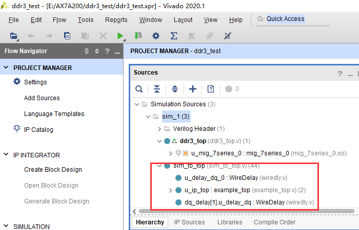
example_top文件例化ddr3_top顶层后,sim目录如下图所示,可以看到ddr3_top和mig控制器都例化进去了

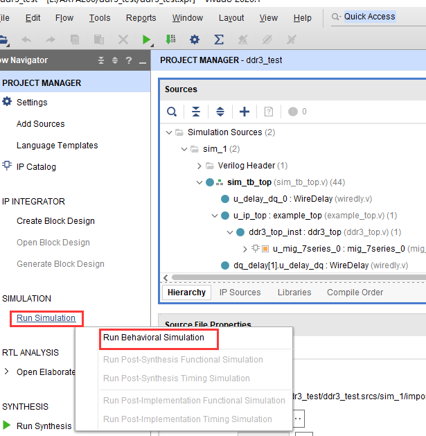
点击run simulation运行ddr3仿真
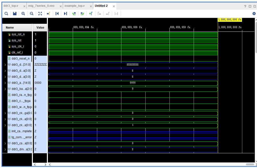
仿真界面如下图所示

选择clk_ref_i的下面所有文件
右击选择Delete删除

删除后,如下图所示
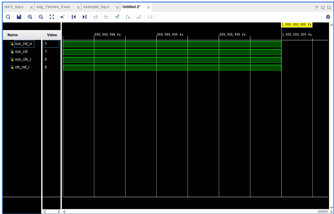
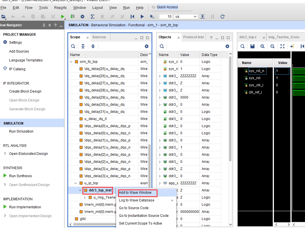
在仿真目录找到我们的顶层文件,右击选择Add to Wave Window,加入到仿真界面
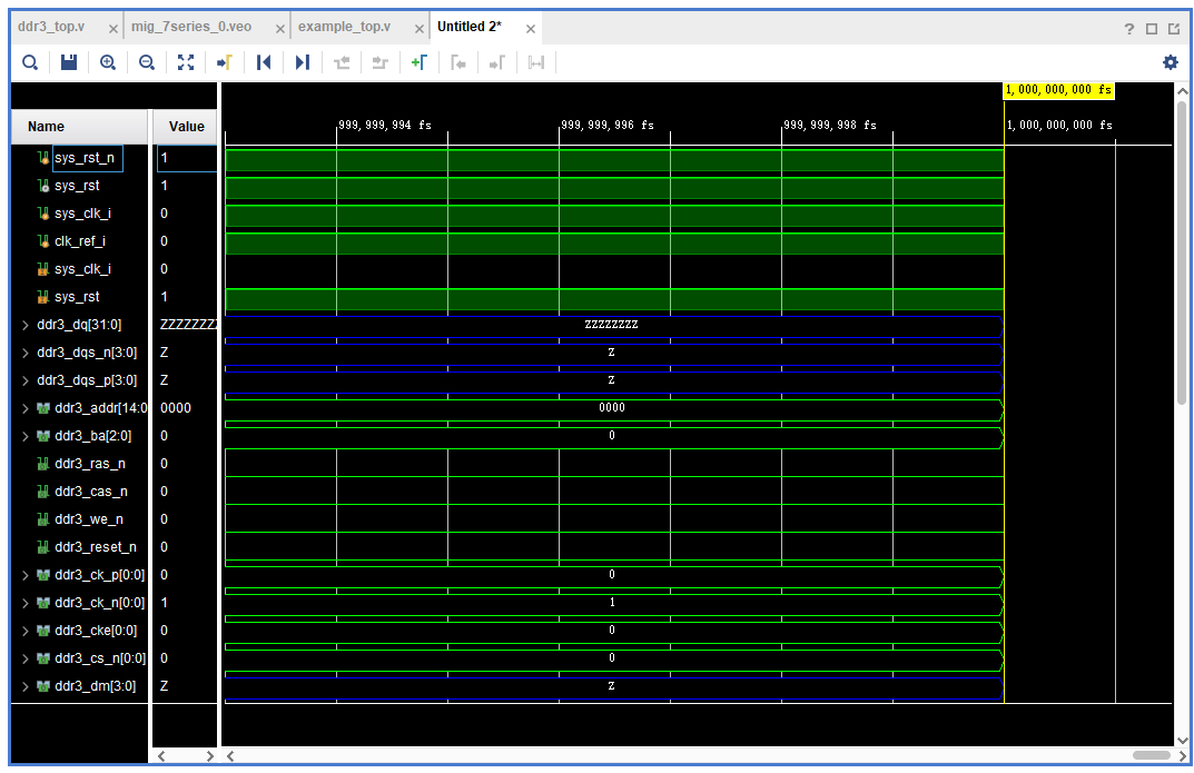
加入顶层后,仿真界面如下图所示
点击复位图标将仿真数据都清零
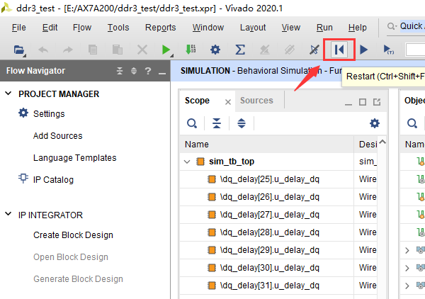
点击复位后,仿真界面如下图所示
点击Run图标开始进行仿真
仿真进行中,初始化时间有点长,继续等待
可以看到,仿真运行到107us后init_calib_complete信号拉高,说明ddr3初始化成功,同时也说明ddr3仿真环境搭建成功
大家可以对比一下在vivado中和modelsim中仿真速度,很明显modelsim中要快很多,那是因为vivado中是直径对mig控制器进行仿真,而modelsim中有点类似对ddr3的仿真模型进行仿真,所以modelsim中仿真较快,而且vivado仿真环境是占用内存的,所以不能仿真太长时间,modelsim中这些方面比vivado要好很多。
vivado中ddr3仿真平台搭建目前已经完成,下一步就是进行一个突发长度的读写。
如若转载,请注明出处


![《Python程序设计(第3版)》[美] 约翰·策勒(John Zelle) 第 9 章 答案](https://img-blog.csdnimg.cn/de24d16fb1c3466ba833ce4af4eb6d9a.png)