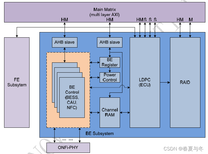
FE: Cortex-R4 处理器 第一个基于 ARMv7-R 体系结构的深层嵌入式实时处理器
BE : Cortex-M3处理器 基于 ARMv7-M体系结构
The YuTu SoC is a Flash memory controller chip, which provides a PCIe Gen 3x4 host interface and 4 channels (up to 8 CEs per channel) Flash interface.
BE subsystem
There are two important data structures in BE subsystem.
One is Link List structure, which is used to exchange data with FE/firmware.
The other is BESS command structure, which is used to exchange data with firmware.
BESS: Back-end Sequence Scheduler(which is a module in BE)
BESS把BESS命令发给CAU, CAU来调度它们
三个status FIFO
status_fifo for those BESS commands, which have been executed correctly,
error_fifo for those BESS commands, which have error(s).
bdcu_error_fifo for the BDCU decode error status
descriptors: descriptors in one command queue are executed in order
command queue: 32bit width and 64 depth
FIFO: 32bit width and 64 depth
command chain:
link list structure: used to exchange data with FE/firmware
BESS command structure: used to exchange data with firmware
context RAM: 32-bit width and 10 depth, in which the parameters of one NFC command is stored. The context RAM is released when NFC command is finished
status FIFO:
error FIFO:
Both NFC and BDCU returns command status to BESS, the successful command status is returned in status FIFO, and error command status is returned in error FIFO
AHB: Advanced High-performance Bus.AHB-32 means 32-bit width AHB bus.
APB: Advanced Peripheral Bus
AXI: Advanced extensible Interface bus.AXI-32 means 32-bit width AXI bus.
TCM: Tightly-Coupled Memory
NVIC: Nested Vectored Interrupt Controller.
PLL: Phase Locked Loop.
MUX: Multiplexer
SRAM: Static Random Access Memory
DDR: Double Date Rate SDRAM
SSD: Solid State Drive
LUN: Logical Unit Number
Plane: The unit consists of a number of Flash blocks.There are one or more Planes per LUN.
IP: Intellectual Property
IP核: intellectual property core(知识产权核),指某一方提供的、形式为逻辑单元、芯片设计的可重用模块
AES: Advanced Encryption Standard. AES-XTS is a mode of AES
BCH: BCH is a kind of cyclic error-correcting codes.
The acronym BCH comprises the initials of the inventors’ names
RS: Reed -Solomon
NVMe: Non-Volatile Memory Express
YuTu: The SoC name, which is an SSD controller SoC
FLBA: Flash LBA
IPC: Inter-Processor Communication
EDMAC: Enhanced DMA Controller
NFC NAND Flash Controller, which sends/receives data to/from NAND flash
MT: Micro-code Table
NCCU: NFC Context Control Unit
NPP NAND protocol processor
Microcode: a sequence of NPP commands
Context: parameters are paired with a microcode
CAU: command accelerate unit
CAU is responsible for issuing and scheduling commands to NFC, LDPC AND Channel RAM
CC: command condition
CF: command fetch
CHRAM: channel RAM
DCU: data compare unit
GPR: general purpose register
IMM: immediate number
LSB: least significant byte
MSB: most significant byte
NI: NAND interface
NSR: NPP status register
ONFI: open NAND flash interface
PC: program counter register
RA: register address
RBO: register byte offset(2bit)
REG: register
CTI: Cross-Trigger Interface
CTM: Cross-Trigger Matrix
DAP: Debug-Access Port
ETM: Embedded Trace Macrocell
JTAG: Joint Test Action Group
TRNG: True Random Number Generator
OTP: One-Time Programmable
HLBA: Host LBA
CGE: Command Generation Engine
DDP: DDR Data Protection
PMU: Power Management Unit
TCON: Timing Controller
Interrupt Control
VIC:Vectored interrupt controller
Channel Ram
Overview
The Channel Ram module of the back end part is responsible for supplying the data for NFC module for program operation.
And this module is responsible for supplying the data from BDCU module for reading operation.
The Channel Ram module is controlled by the CAU module.
Before the command is sent the BDCU or NFC module, the CAU module checks the status of Channel Ram firstly. According to the status of the Channel Ram, the CAU send the commands to the BDCU module and NFC module.
The AHB can write and read the registers and SRAM.
Feature Overview
This module should support 4 channels for program. Each channel could store 2 buffers data.
This module should support 4 channels for reading. Each channel could store 5 buffers data.
This module should support 1 channel for two-bits hard-decoding. The channel could store 2 buffers data.
BDCU Back end Data (path) Control Unit
LDPC low density parity check code include ECC、ECU etc.
CRC: Cyclic Redundancy Check(循环冗余码校验)
ECC: Error Correction Control
RAID Redundant Arrays of Independent Disks.
The RAID module of the backend part is responsible for the RAID system for the data between SOC and the FLASH
The RAID module takes the responsibilities of generating RAID parity for NAND Flash data.
RAID module is connected to LDPC module.
There are two group interfaces, one is for write (program)data to NAND Flash, the other is for read data from NAND Flash.
The page has an extra parity per RAID stripe, and the page parity s an XOR result from all pages belong to the stripe.Page_PARITY = Page_1 ^ Page_2 ^ Page_3 ^ … ^ Page_n . This means the firmware can reconstruct only one failed page by reading all of the other pages.
RAID ID: strip_id
encoder flash的数据(不带异或结果)添加异或结果后返回
Writing Data
decoder flash的数据有误时,通过异或结果和其它数据恢复错误的数据
Reading Data
Libra
Data Format in data path
SQ Submission Queue
CQ Completion Queue
doorbell通信
DOORBELL FUNCTION OPERATION:
1.doorbell configuration
To use the doorbell, user should follow steps:
2.submission doorbell
Firmware dispatch command to hardware engine by submission doorbell interface. The submission queue setting steps are:
3.completion doorbell
CPU Receives CQ Flow
typedef struct
{
u32_t status; //–> error status.
u32_t hw_base; //–> hard-ware base address.
DB_QSTS_t *pQStatus;
DB_QCTRL_t *pQCtrl;
DB_QINFO_t *pQInfo;
u32_t wptr; //–> write pointer
u32_t rptr; //–> read pointer
}DB_QUEUE_HANDLE_t;
ADM advanced data management
ADM is mainly responsible for transferring data between FE and BE module, get wtag/rtag from CPU1, and send lbn ready, wtag ready, wtag done to CPU1 by doorbell.
LBN Logical Block Number, one LBN is 4KB
Wtag one Wtag stands for one page, Now the one page is 16KB.(TBD).
Rtag one Rtag stands for one LBN
Wtag Management
In ADM thread, ADM will get wtag from CPU doorbell, and then save the wtag. ADM will create 512 wtags structure to save the wtag number.
Rtag Management
ADM get the rtag,lbn,ctag from doorbell, and need to save the information.
Central Buffer
Central buffer is used to save the write data from FE, one wtag stands for one page(16KB).
DDR Read Buffer
DDR read buffer is used to save the read data from BE, one rtag most stands for one page(16KB).
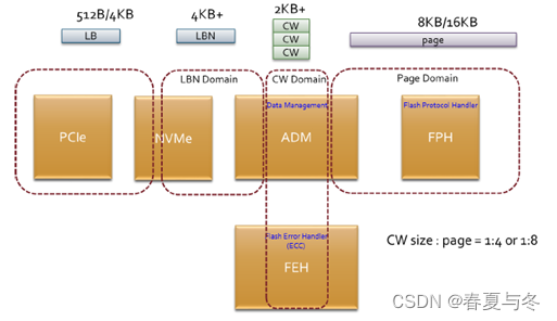
The ADM block is an Advanced Data Management. It’s placed at the central of the whole chip’s dataflow. The main function of ADM is to do data format translation, and handles the data flow between neighbor blocks.
There are three kinds of data format co-exist in ADM,
(1) LBN 4K domain
(2) CW 2KB+ domain (Code Word (2k))
(3) page 8KB/16KB domain
For easy to manage and identify the data for transmission, 512 tag numbers are used to label each segment of data, and communicate with other HW blocks. The central SRAM is about 1.5MB, for temporally data storage.
The block has the following features:
1.Auto handshake between front-end and back-end
2.Handle ECC flow
3.LBN to CW transfer
4.Handle FW L2P backup/restore from/to DDR
5.Hardware automatically to get and release the central SRAM space
6.512 wtag number shared by all kinds of write operation
7.512 rtag number shared by all kinds of read operation
8.1.5 MB central SRAM. All accessible by CPU with 4byte aligned address
FUNCTION OPERATION
HOST Write Flow
When doing host write traffic, the host control block is to receive command and data for the LBN data comes from PCIe to NVMe then to ADM. The data length of one LBN is 4K byte, along with a dedicate LBN number. ADM block will translate into CW domain with 2K+ byte length. The length of a CW depends on the code rate setting related to LDPC.
After one CW is ready in central SRAM, the FEH_CTRL block will get CW data and send to FEH encode path. One CW after the other. Then FEH will send back the CW data, followed by the LDPC encode parity. ADM will temporally store these encoded data into SRAM, until 8 CWs(assume page is 16K) are all ready in SRAM, the complete page data will get by FPH, then write into FLASH.
During the write path, a wtag number is assigned by FW to ADM and FPH, for labeling the whole page data. So the hardware blocks communicate with the same wtag number for data transmission.
HOST Read Flow
The traffic of host read is reversed. FW sets the rtag to ADM and FPH. FPH get multiple CWs related to the same rtag from FLASH, then write to ADM. Then ADM will send each CW to FEH decode path, for LDPC decoder check and correct the CW data. One after the other. ADM will compound the LBN 4K data from these CWs, then inform NVMe for LBN data is ready.
DDR Path Control
The DDR path control is mainly for FW to store the L2P table from DDR to FLASH. Or from FLASH to DDR for table rebuild. These DDR data will also translate into CW domain, do FEH encode, then to page domain.
FEH flash error handler
FEH is in charge of the whole error correction of the system. It is mainly separated into two parts, decoding parts and encoding parts.
FEH mainly do two things, encoding a ~2KB data to generate the code word with parity to protect the data and decoding the code word with errors to recover the original data.
FUNCTION OPERATION
decoder
it mainly contains 3 majors, which are ldec input control, ldec core, and ldec output control.
As its name, the ldec input control module is in charge of the input management including decoding header information which gives the required individual information of the input code word, doing padding for the input data, and collecting and doing mapping the soft value data when the input data is soft-bit data.
encoder
It mainly contains 3 major parts, which are lenc input control, lenc core, and lenc output control.
FPH flash protocol handler
This block handles the flash protocol to access the flash.
Flash access is CodeWord(CW) base.
FUNCTION OPERATION
Door-Bell Command Interface
The CPU access the AXI bus & Internal DCCM memory have different latency. So FPH use the door-bell interface to send command & send completion to reduce the CPU access latency.
Pure IO (PIO)
Firmware directly controls the Flash interface by setting registers PIO_CMD, PIO_ADDR and PIO_DAT to access NAND Flash.
Flash Command Unit (FCU)
The flash command sequence is defined by Flash Command Unit (FCU). Firmware defines the FCU sequence and stored it in Internal RAM (IRAM). By specifying the FCU staring pointer through MTC table, hardware automatically executes that FCU sequence until sequence ends.
Macro Task Command (MTC)
MTC stands for Multi-Task Command. By using this mode, Firmware can call the FCU sequences by send MTC.
Each MTC entry is 32-byte including one FCU pointer & Tag.
Total have 512 entry MTC for Firmware to trigger FCU execution. Hardware automatically executes the MTC in parallel across different CEs.
FPH Door Bell Program Sequence:
Step 1 : Submission Queue setting and Completion Queue setting
Step 2 : Put the command setting into DCCM1.
Step 3 : Set SQ Write Pointer Increase Unit
Step 4 : Check CQ empty or not. (FPH HW will put a status information to the CQ)
Step 5 : Get status information from the CQ, and analyze result of the command operation. If CQ is not empty, FW continually reads information from CQ.
DMAC Direct Memory Access Controller
DMAC is mainly responsible for transferring data between DDR and ADM module, DAMC get physical/cluster write/read command from CPU1, then write data from DDR to ADM or read data from ADM to DDR.
The DMAC stands for Data Memory Access Controller used to accelerate the data movement between RAM as well as data calculation Firmware needs to perform.
The Firmware sends a command to DMAC via DoorBell by initializing the SQ (Submission Queue) and CQ (Completion Queue), then DAMC fetches command from SQ, executes it, and sends command status to CQ.
FUNCTION OPERATION
The DMAC supports these commands:
- COPY
The copy operation performs data copy from source address to target address with a specific data length. The COPY command is issued by CPU via the Doorbell. The content of CQ status indicates the operation finish of the copy command. - Set Value
- Compare
The Compare operation is to compare data content between two source addresses with a defined length. The DMAC engine will stopped and report compare error if any data mismatch is detected for saving the execution time. The offset of data mismatch address is reported to CPU via Doorbell CQ.
4.XOR, XNOR, OR
ONFi
DDR : Acronym for double data rate.
SDR : Acronym for single data rate.
Address :
The address is comprised of a column address with 2 cycles and a row address with 3 cycles.
The row address identifies the page, block and LUN to be accessed.
The column address identifies the byte within a page to access.
The least significant bit of the column address shall always be zero.
Column Address : The byte location within the NAND flash page register.
Row Address : Refer to the block and page to be accessed in NAND flash memory
Page : The smallest addressable unit for the Read and the Program operations.
WL : Word line. The WL contains three pages and could be selected by raw address for Read or Program operation in TLC device.
Block : Consists of multiple pages and is the smallest addressable unit for the Erase operation.
Page register : Register used to transfer data to and from the Flash Array.
Defect area : The defect area is where factory defects are marked by the manufacturer. Refer to the “Factory Defect Mapping”.
Device : The packaged NAND unit. A device may contain more than a target.
LUN (Logical Unit Number) : The minimum unit that can independently execute commands and report status. There are one or more LUNs per CE.
Target : An independent NAND Flash component with its own CE signal.
SR[x] (Read Status) : SR refers to the status register contained within a particular LUN. SR[x] refers to bit x in the status register for the associated LUN. Refer to “Read Status Operation” for the definition of bit meanings within the status register.
Word:A word is sixteen (16) bits of data. A word may be represented as 16 bits or as two adjacent bytes.
O/M:O/M stands for Optional/Mandatory
PIN: 引脚,从集成电路(芯片)内部电路引出与外围电路的接线,所有的引脚就构成了这块芯片的接口
LBA:Logical Block Address
PBA:Physics Block Address
SSD的主控制器是使用LBA和PBA的映射表来管理闪存的(通过FTL实现)
FTL:Flash translation layer 物理地址逻辑地址之间的转换
复位: reset
NPP command
0x0 OPC_SEND_CMD_ADDR send command/address
is used by FW to send the Flash command or address.
OUTPUT:
TO NI
NO TO CAU
0x1 OPC_NAND_DATA_WR Nand data write
is used to define the write data transfer of the Flash. One write data transfer
maybe has several OPC_NAND_DATA_WR operation codes.
OUTPUT:
TO NI
NO TO CAU
0x2 OPC_NAND_DATA_RD Nand data read
is used to define the read data transfer of the Flash. One read data transfer maybe has several OPC_NAND_DATA_RD operation codes.
OUTPUT:
TO NI
NO TO CAU
0x3 OPC_WRI_REG write register
is use to assign the immediate value to the register. One register maybe need two OPC_WRI_REG operations at most because we just have two byte immediate value and the register have four byte.
OUTPUT:
NO TO NI
NO TO CAU
0x4 OPC_JUMP Jump
is used by FW to control the sequence to implement some condition control like if…else, for loop, while loop or call subroutine/return etc.
OUTPUT:
NO TO NI
NO TO CAU
0x5 OPC_DELAY Delay
is used by FW to insert delay sequence or Flash interface.
OUTPUT:
TO NI
NO TO CAU
0x6 OPC_CRI Compare register with immediate value
is used by FW to insert delay sequence or Flash interface.
OUTPUT:
NO TO NI
NO TO CAU
0x7 OPC_TS thread switch
is used to switch the thread. NPP will hold the current thread and polling other DIE’s available thread and find one to execute it.
OUTPUT:
NO TO NI
TO CAU
0x8 OPC_NOP NOP
OUTPUT:
NO TO NI
NO TO CAU
0x9 OPC_COPY_REG copy register to register
is used to copy one register’s value to another register.
OUTPUT:
NO TO NI
NO TO CAU
0xa OPC_REG_OP register operation
is used to do some arithmetic/logic operation between the register or register with immediate value.
OUTPUT:
NO TO NI
NO TO CAU
0xb OPC_LOAD_CTX load context
is used to load the context data from context RAM to context register
OUTPUT:
NO TO NI
NO TO CAU
0xc OPC_WFE wait for event
OUTPUT:
NO TO NI
TO CAU
0xd OPC_SDT stop flash bus toggle
is used to terminate one Toggle Flash command.
OUTPUT:
TO NI
NO TO CAU
Nand Flash引脚(pin)功能说明
I/O0 ~ I/O7:用于输入地址/数据/命令,输出数据
DQ[7:0]:DATA INPUTS/OUTPUTS。 The DQ pins are used to input command, address and data, and to output data during read operations. The DQ pins float to high‐z when the chip is deselected or when the outputs are disabled.
DQS:Data Strobe signal 。Data output is aligned with DQS falling/rising edge, and data inputs at DQS falling/rising
R/B# :Ready/Busy Output,就绪/忙,主要用于在发送完编程/擦除命令后,检测这些操作是否完成,忙,表示编程/擦除操作仍在进行中,就绪表示操作完成.
CLE:Command Latch Enable,命令锁存使能,在输入命令之前,要先在模式寄存器中,设置CLE使能
ALE:Address Latch Enable,地址锁存使能,在输入地址之前,要先在模式寄存器中,设置ALE使能
CE#:Chip Enable,芯片使能,在操作Nand Flash之前,要先选中此芯片,才能操作
引脚上灰色的阴影:代表我们不需要关心这段时期这些引脚的电平
RE#:Read Enable,读使能,在读取数据之前,要先使CE#有效。
WE#:Write Enable,在写取数据之前,要先使WE#有效。
WP#:Write Protect
Vcc:Power, VCC is the power supply for device.
VccQ:DQ Power, The VccQ is the power supply for input and/or output signals.
Vss:Ground. 接地
VssQ:DQ Ground.The VssQ is the power supply ground.
Vpp:EXTERNAL HIGH VOLTAGE. The high voltage power may be used to improve power efficiency.
VREF:Voltage Reference. VREFQ This signal is used as an external voltage reference for input and DQ signals when VccQ 1.8V is selected. VREF must be used when data inputs/outputs is the speed of 400Mbps and over.
NC:Non-Connection, 未定义,未连接
NU:NOT USABLE
AC:Alternating Current
DC:direct current
RE:头上有个横线,说明此RE是低电平有效
RE# 为了书写方便,在字母后面加“#”,也是表示低电平有效
如果字母头上啥都没有,就是默认的高电平有效
(NAND Flash)有多种结构.下面内容针对三星的K9F1208U0M)每页528Bytes(512byte(Main Area)+16byte(Spare Area)),每32个page形成一个Block(32528B)。具体一片flash上有多少个Block视需要所定。我的具有4096个block,故总容量为4096(32*528B)=66MB,但是其中的2MB是用来保存ECC校验码等额外数据,故实际中可使用的为64MB。
Memory Operation
basic command sets
page read
sequential cache read
read start for last page cache read
random cache read
one shot program
one shot cache program
block erase
read for copy-back
copy-back program
random data input
random data output
set features
get features
read ID
read status
reset
reset LUN
half page read


