Meint Smit et al 2014 Semicond. Sci. Technol. 29 083001
9.通用测试
9.1. 晶圆验证
在通用工艺中,必须对每批次晶片的工艺性能进行验证;客户将期待这样的验证。在MPW中,验证用户ASPIC工艺性能是不实际的;每个ASPIC都需要不同的测试设置和程序,ASPIC的失败并不意味着工艺失败,问题也可能出现在用户设计中。验证通用过程的唯一实用方法是包括用于BBB表征的测试单元。如果BBB的性能是可以的,那么基于这些BBB的所有元件的性能也应该是可以的——如果它们设计得当,并且流程足够成熟。通过将测试限制在BBB上,我们避免了最终出现大量构建块,而这些构建块的测试将需要不切实际的大测试单元。此外,对于工艺技术开发来说,聚焦在一小组BBB是可行的,工艺优化可以集中在这些BBB上。
9.2. 晶圆上测试
测试光学元件比测试电气元件更困难。首先,光端口只有在晶片被切割后才可接近,其次,光在波导中或波导外的精确耦合的对准公差要求很高,因此测试很慢。电测量的对准公差容限更大,因为只要接触良好,电气触点就可更大,一些未对准的影响就很小。电测量的一大优点是可以在晶圆上进行:不需要对晶圆进行切片测试,这使得自动化测试更加容易。
因此,我们正在研究对光子IC中最重要的构建块的光学特性进行晶圆上测试的可能性。在PARADIGM项目中,我们正在研究两种方法:一种是在芯片中集成垂直输出耦合器,垂直光学探针可以访问该耦合器。另一种方法是将待测器件(DUT)与源和检测器集成在一起。在后一种方法中,我们将测试光路(即使是复杂的测试光路)添加到ASPIC设计中,这相对简单。我们将在本节中简要介绍这种方法。
测量传输损耗的一般方法是将其与参考器件(通常是直波导部分)的传输进行比较。如图28所示,我们在源和探测器之间集成DUT和参考器件,在假设源相同的情况下,通过比较检测器的输出电流来测量,从而在晶圆上实现这一点。作为一个源,我们可以使用集成的SOA部分,它将生成一个宽的频谱,以便在整个频带上对测量的传输进行平均(加权)。如果我们使用集成DBR激光器作为光源,我们可以在特定波长下进行测量。该方法的准确性取决于集成测试源和检测器的重复一致性。

添加图片注释,不超过 140 字(可选)
Oclaro和COBRA通用集成过程中最重要的BBB是无源波导器件、SOA和相位调制器。它们最重要的特性分别是传输损耗、增益谱和电光效率。为了说明我们的方法,我们将讨论我们目前正在研究的三种结构,以用电探针测量它们。
波导损耗原则上可以通过比较短波导段和长波导段的传输来测量。如果传输损耗较低,则需要长波导段来足够准确地测量损耗,并且测试结构将具有较大的占地面积。另一种方法如图29所示,这基于这样一个原理,即环形谐振器的传输对环中的损耗非常敏感。为了测试波导损耗,我们在带监测二极管的可调谐DBR激光器和检测二极管之间插入一个由MMI耦合器形成的环。通过扫描波长并将检测器电流标准化为监测二极管的电流,我们记录了如图右侧所示的曲线。通过测量最大和最小功率之间的消光比,我们可以确定波导损耗。为了进一步提高测量精度,我们可以比较具有相同曲线但不同直波导段长度的环。

添加图片注释,不超过 140 字(可选)
SOA增益。图30展示了用于测量光放大器增益谱的测试结构。如果SOA1和SOA2相同,则SOA2开启和关闭时SOA1的输出功率之比就是SOA1的增益。以这种方式测量的增益是增益谱上的加权平均值。如果我们在SOA1后面插入AWG,并将光电探测器连接到每个输出端口,我们可以测量AWG的每个波长通道的光谱增益。这将为我们提供如图30中红点所示的采样增益频谱。几个通道就足以充分验证SOA性能。

添加图片注释,不超过 140 字(可选)
电光效率。测量Vπ(相位调制器引入180°相移的电压)的一种简单方法是将其插入源和检测器之间的MZI中,如图31所示,将传输记录为电压的函数。Vπ是两个极小值之间的电压差。通常情况下,它与电压有关,因此需要更复杂的方法来找到ϕ–V曲线。
这三个例子说明了如何使用电探针在晶片上测量光电特性。在图5中,以插图形式出现的放大MPW单元显示了包含如上所述的多个测试结构的测试单元。通过测量BBB的性能并将其与标准进行比较,这种测试单元可用于快速准确地验证晶片。

添加图片注释,不超过 140 字(可选)
10.未来前景
由于在开发基于InP的单片集成和硅光子学的晶圆技术基础设施方面进行了大量投资(在欧洲和国家项目中远远超过5000万欧元),欧洲在建立这种新的工作方式方面取得了重大进展。
10.1. 技术发展
如本文所述,自2007年以来,COBRA已经提供了对第一代(G1)InP研究平台的小规模访问。工艺能力正在逐步提高,目前ASPIC集成了10 Gb /s速度的激光器、光放大器、调制器和检测器以及各种无源光学元件。该平台适用于研究和原型设计,但不适用于批量生产。2009年,EuroPIC项目开始将晶圆模型从大学环境转移到工业和半工业平台(Oclaro和FhG-HHI的晶圆厂),并开始开发软件设计套件和标准化封装解决方案。EuroPIC平台技术的能力列于表2的2012栏。本文第6节介绍了本项目中开发的一些ASPIC。结果非常有希望,JePPIX平台[44]已经开始对这些晶圆工艺进行半商业化访问。预计在2015/16年度向全面商业运营过渡,前提是当时的市场需求证明了这种过渡是合理的。
2010年,PARADIGM项目开始开发第二代(G2)平台,该平台具有改进的功能和性能:能够提供高达40 Gb /s的发射机和接收机功能,提供卓越的激光器和放大器,更宽泛的发射和检测波长以及其他先进功能。该工艺将与先进的特定应用技术相竞争,但入门成本要低得多。表2第2015列列出了其目标属性。此外,该项目设想开发低成本的通用包和具有强大元件库的复杂PDK,如第7和第8节所述。在项目期间,为选定的外部用户提供小规模访问。假设有一个可行的商业案例,预计在2017年左右全面商业运营,并提前进入研发阶段。
一个重要的发展是电和光的单片集成。在硅光子学中,几个小组已经证明了光路在硅衬底上的硅膜中的集成,其中一些还包括激光器等有源光学元件。硅光子学光路中激光器集成的主流是通过在光子硅层顶部结合基于InP的III–V层堆叠,并处理III–V中的激光器和硅层中的其他元件[92–94]。在这种方法中,最终需要三层:
(1) 一个CMOS电子层
(2) 一个硅光子层
(3) 一个InP光子层
两个光子层之间的有效耦合是困难的,并且需要在芯片上具有显著大的区域,尤其是在有源元件变得更小的情况下。COBRA采用了一种方法,将全光子功能集成在单个基于InP的硅上膜(IMOS)中,从而通过消除硅光子层和两个光子层之间的耦合问题将层数减少到两个[95]。该技术可以在CMOS晶圆厂(具有专用工艺线)中实现,也可以在InP晶圆厂中实现。它可能成为将InP光子学与硅电子技术相结合的第三代(G3)晶圆技术。
10.2. 成本发展
人们普遍认为,InP PICs比硅光子PICs贵得多。通过应用通用晶圆模型,InP PIC的研发和原型制作成本可以降低一个数量级以上,这使得InP PIC与硅光子非常有竞争力。目前,JePPIX(www.JePPIX.eu)为基于InP的晶圆工艺提供MPW运行的半商业访问,ePIXfab(www.ePIXfab.eu)和OpSIS(www.opsisfoundry.org)为硅光子提供半商业访问。为了进行比较,所提供的功能和性能以及每平方毫米设计面积的成本是最相关的数字。交付的芯片数量也可能是相关的,但通常在第一阶段,测试新设计只需要几个芯片。如果我们将最先进的硅光子工艺与最先进的基于InP的工艺进行比较,我们会发现在MPW运行中,InP以更低的成本提供了更多的功能(激光器、光放大器和更好的调制器),无论MPW的价格还是平方毫米的价格。
对于这两种技术,小规模生产和原型设计的成本将由非共享成本主导,无论是晶圆工艺、PDK和IPB、模型开发、表征、软件开发,还是最终用户特定的芯片设计时间和资源。在这里,InP似乎具有优势,因为大规模CMOS晶圆厂的研发成本明显高于小型InP晶圆厂,这使得通用InP技术的入门成本低于硅光子学技术。对于批量生产,InP晶圆的每平方毫米成本肯定高于硅光子学,这主要是由于使用的衬底晶圆较小,生产量较小。目前,它们在10-20€/mm2的范围内,但一旦晶圆厂获得更高的订单,这一成本就会减少。由于硅光子学需要更高的研发投资,InP在小批量甚至中批量生产方面可能具有竞争优势。
为了与硅光子学进行公平的比较,我们还必须在比较中包括封装成本。在目前的光子封装技术中,封装成本明显高于芯片成本,因此对于最终产品来说,芯片的价格不如集成在芯片中的功能重要。由于InP还集成了大多数应用中所需的激光器和光放大器,因此封装成本将低于硅光子芯片,在硅光子芯片中,激光器必须以更昂贵的混合方式集成。因此,我们预计,尽管封装的InP PICs的平方毫米价格更高,但与封装的硅光子PICs相比,它将极具竞争力。
10.3. 应用
预计研发时间和芯片制造成本的大幅减少将导致PIC在光子元件市场的份额大幅增长。到目前为止,PICs的商业部署主要局限于电信核心网络应用的特定领域,在这些领域,它们的功能无法与竞争技术相匹配。电信是光子技术开发的一个相对小众的领域,约占全球光子市场的5%[96]。尽管如此,电信业的严格要求正在推动PIC研究。因此,在其他已建立的光子市场中利用PIC技术的机会是巨大的,如光纤传感器解调 单元、医疗诊断、计量以及当今光子学无法提供有竞争力的价格水平的许多应用。在第6节中,讨论了在这些市场中应用的一些ASPIC。
通用晶圆方法的另一个重要优势是上市时间短。因为ASPIC是在合格的晶圆工艺中开发的,所以升级到更大的生产量是直接的:一旦ASPIC设计满足用户要求,用户就可以在开发ASPIC的同一工艺中订购许多晶圆,现在他可以完全用自己的设计来填充这些晶圆。对于设计面积为4×5 mm2的ASPIC,单个3’晶片将包含100多个芯片。因此,用1000个晶片可以获得10万个芯片的体积,这可以由中型InP晶圆厂轻松处理。
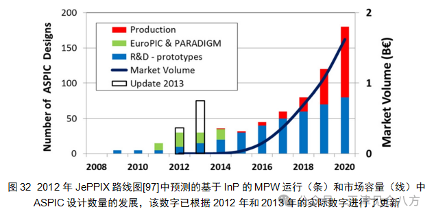
图32显示了2012年JePPIX路线图[97]中发布的基于InP的ASPICS实现的市场发展预测。它是基于MPW运行中开发的ASPIC数量的预期增长。在图中,标有“2013年更新”的条形图表示2012年和2013年的实际数字,远高于2011年绘制该图时的预期。这一急剧增长的部分原因是,PARADIGM项目提供的用户数量远高于最初的预期,而2014年的预期将更低。然而,我们预计2014年半商业接入的可用性将弥补这一减少。
添加图片注释,不超过 140 字(可选)
在JePPIX路线图模型中,预测的市场发展是由大量具有高附加值的中小型应用引起的,而不是由少数低成本的“杀手级”应用引起。该模型为更大的市场容量提供了一条进化之路,这将使晶圆厂能够在一些较小的步骤中提高性能并降低制造过程的成本。这样的成本降低最终也可以实现在大众市场中的低成本应用。

11.结论
基于InP的通用晶圆技术将大大降低有兴趣在新产品或改进产品中应用InP ASPIC的公司的进入成本。它将为许多中小企业带来先进的基于光子InP的集成技术。欧盟和各国政府的重大研发资金使晶圆方法达到了一个水平,即实验性晶圆运行已在工业集成平台上成功演示,晶圆平台的半商业化接入已于2014年开始。在PKD的开发和封装的标准化方面已经取得了重大进展,目前InP PDK支持的元件库比任何其他开放访问的光子集成技术都强大得多。
除了原型设计贯穿多项目晶圆服务之外,我们预计InP在中小型生产方面将极具竞争力。由于生产基础设施的性质,与先进的硅光子学工艺相比,启动成本更低,同时提供了更多的功能。从长远来看,我们预计InP Photonics和CMOS电子器件将合并为异构集成技术,其中CMOS将提供电子功能,InP将提供光子功能。
术语
ADS Advanced Design System (Agilent)
API application programming interface
ASIC application specific IC
ASPIC application specific photonic IC
ASPIC ™ Advanced Simulator for Photonics Integrated Circuits (Filarete)
AWG arrayed waveguide grating
BB building block (used for both BBB and CBB,where the distinction is not relevant)
BBB basic building block
BPM beam propagation method
BOTDR brillouin optical time domain reflectometry
BCB benzocyclobutene
BTB basic technology block
CBB composite building block
CMOS complementary metal–oxide–semiconductor
CMRR common-mode rejection ratio
COBRA Communication technologies; Basic Research and Applications (TU/e research institute)
DBR distributed Bragg reflector
DFB distributed feedback laser
DI delay interferometer
DQPSK differential quadrature phase shift keying
DRC design rule checking
DS downstream
DUT device under test
DUV deep ultra-violet (193 nm)
EAM electro-absorption modulator
E-beam electron-beam
EI electrical isolation section
EME Eigen-mode expansion
e-o electro-optical
ERM electro-refractive (phase) modulator (depletion-type)
ERMI electro-refractive (phase) modulator (injection-type)
ePIXnet European Network of Excellence on Photonic Integrated Components and Circuits,
EuroPIC European manufacturing platform for PhotonicIntegration Circuits
FDTD finite difference time domain
FET field effect transistor
FMW fibre matched waveguide
FP Fabry–Perot
FSR free spectral range
Ge germanium
InGaAs Indium gallium arsenide
InGaAsP Indium gallium arsenide phosphideIC integrated circuit
IIR infinite impulse response
IMOS InP membrane on silicon
InP indium phosphide
IO input–output
IOP PD IOP photonic devices (IOP = Dutch InnovationResearch Project)
IP intellectual property
IPB IP-block
JePPIX Joint European Platform for Photonic Integration of Components and CircuitsLSI large scale integration
MEMPHIS Merging Electronics and Micro and nano Photonics in Integrated Systems, Dutch SmartMix project
MMI multi-mode interference
MFD mode field diameter
MI Michelson interferometer
MIR multimode interference reflector (MMIReflector)
MOVPE metal-organic vapour-phase epitaxy
MPW multi project wafer
MQW multi quantum well
MZI Mach–Zehnder interferometer
OCT optical coherence tomography
PARADIGM Photonic Advanced Research and Development for Integrated Generic Manufacturing
PCB printed circuit board
PD photo detector
PDA photonic design automation
PDK process design kit
PHASAR phased array (early name for AWG)
PIC photonic integrated circuit
PM-DQPSK polarization multiplexing differential quadrature phase-shift keying
POSA PIC optical sub-assembly
PR Polarization rotation section
QD quantum dot
QW quantum well
ROSA receiver optical sub-assembly
RR ring resonator
R&D research & development
SA saturable absorber
SAG selective area growth
SEM scanning electron microscope
Si silicon
SFDR spurious-free dynamic range
SME small or medium enterprise
SOA semiconductor optical amplifier
SOI silicon on insulator
SSC spot size convertor
SSMF standard single mode fiber
STW GTIP Generic Technologies in Integrated Photonics, STW Perspectief Project (STW = Dutch Technology Foundation)
TBR tunable Bragg reflector
TE transverse electric (field)
TEC thermo-electric cooler
Ti-Pt-Au titanium-platinum-gold (contact)
TM transverse magnetic (field)
TOM thermo-optic modulator
TOSA transmitter optical sub assembly
US upstream
VLSI very large scale integration
WDM wavelength division multiplexing
WG waveguide (passive)
WGS deep etched waveguide (strong confinement)
WGT waveguide termination
WGW shallow etched waveguide (weak confinement)
XFP 10 gigabit small form factor pluggable module
参考文献
[1] Miller S E 1969 Integrated optics: an introduction Bell Syst. Tech. J. 48 2059–69
[2] Tien P K 1977 Integrated optics and new wave phenomena in optical waveguide Rev. Mod. Phys. 49 361–420
[3] Koren U et al 1989 WDM light source with integrated QW tunable lasers and optical amplifier Appl. Phys. Lett. 54 2056–8
[4] Cremer C 1991 Grating spectrograph in InGaAsP/lnP for dense wavelength division multiplexing Appl. Phys. Lett. 59 627–9
[5] Duthie P J et al 1991 Guided wave switch array using electrooptic and carrier depletion effects in indium phosphide Electron. Lett. 27 1747–8
[6] Gustavsson M et al 1992 Monolithically integrated 4 × 4 InGaAsP/InP laser amplifier gate switch arrays Electron. Lett. 28 2223–5
[7] Kaiser R 1994 Monolithically integrated polarization diversity heterodyne receivers on GaInAsP/InP Electron. Lett. 30 1446–7
[8] Smit M K 1988 New focusing and dispersive planar component based on an optical phased array Electron. Lett. 24 385–6 [9] Takahashi H et al 1990 Arrayed-waveguide grating for wavelength division multi/demultiplexer with nanometer resolution Electron. Lett. 26 87–8 [10] Dragone C 1991 An N × N optical multiplexer using a planar arrangement of two star couplers IEEE Photon. Technol. Lett. 3 812–5
[11] Amersfoort M R et al 1993 High performance 4-channel PHASAR wavelength demultiplexer integrated with photodetectors Proc. 19th Eur. Conf. Opt. Comm. (ECOC‘93) Post deadline Papers (Montreux, Switzerland, September 12–16) vol 3 pp 49–52
[12] Zirngibl M et al 1995 WDM receiver by monolithic integration of an optical preamplifier, waveguide grating router and photodiode array Electron. Lett. 31 581–2
[13] Steenbergen C A M et al 1996 Compact low loss 8 × 10 GHz polarization independent WDM receiver 22nd Eur. Conf. on Opt. Comm (ECOC’96, Oslo) vol 1 pp 129–32
[14] Zirngibl M and Joyner C H 1994 12 frequency WDM laser based on a transmissive waveguide grating router Electron. Lett. 30 701–2
[15] Zirngibl M et al 1996 An 18-channel multifrequency laser IEEE Photonics Technol. Lett. 8 870–2
[16] Staring A A M et al 1996 A compact nine-channel multiwavelength laser IEEE Photonics Technol. Lett. 8 1139–41
[17] Zirngibl M and Joyner C H 1994 High performance, 12 frequency optical multichannel controller Electron. Lett. 30 700–1
[18] Ishii H et al 1998 Monolithically integrated WDM channel selectors on InP substrates Proc. 24th Eur. Conf. Opt. Comm. (ECOC’98) (Madrid, Spain, 20–24 September) pp 329–30
[19] Ménézo S et al 1999 10-wavelength 200 GHz channel spacing emitter integrating DBR lasers with a PHASAR on InP for WDM applications IEEE Photonics Technol. Lett. 11 785–7
[20] Mestric R et al 2000 Sixteen-channel wavelength selector monolithically integrated on InP Proc. Opt. Fibre Comm. Conf. (OFC 2000) (Baltimore, March 2000) 81-83
[21] Kikuchi N et al 2001 Monolithically integrated 64-channel WDM channel selector on InP substrate Proc. 27th Eur. Conf. on Opt. Comm. (ECOC’O1) (Amsterdam) pp 4–5
[22] Herben C G P et al 1999 Polarization independent dilated WDM cross-connect on InP IEEE Photonics Technol. Lett. 11 1599–601
[23] Chandrasekhar S et al 1995 Monolithic eight-wavelength demultiplexed receiver for dense WDM applications IEEE Photonics Technol. Lett. 7 1342–4
[24] Tolstikhin V I 2003 44-channel optical power monitor based on an Echelle grating demultiplexer and a waveguide photodetector array monolithically integrated on an InP substrate Proc. Opt. Fibre Comm. Conf. (OFC 2003) Post Deadline Paper PD37-1 (Atlanta, GA, USA, March 23–28)
[25] ASIP/Three-Five Photonics 2004 (www.rle.mit.edu/cips/ conference04/Pennings_ASIP.pdf)
[26] Nagarajan R et al 2005 Large-scale photonic integrated circuits IEEE J. Sel. Top. Quant. Electron. 11 50–65
[27] Nagarajan R et al 2006 Single-chip 40-channel InP transmitter photonic integrated circuit capable of aggregate data rate of 1.6 Tbit /s Electron. Lett. 42 771–3
[28] Nicholes S C 2009 The world’s first InP 8 × 8 monolithic tunable optical router (MOTOR) operating at 40 Gbps line rate per port Opt. Fibre Com (OFC 2009) Postdeadline Paper PDPB1 (San Diego, CA, USA, 22–26 March)
[29] Wang H, Wonfor A, Williams K A, Penty R V and White I H 2009 Demonstration of a lossless monolithic 16 × 16 QW SOA switch Proc. 35th Conf. on Optical Comm. (ECOC 2009) Post-deadline Paper (Vienna, 20–24 September)
[30] Soares F M 2010 Monolithically integrated InP wafer-scale 100-channel × 10 GHz AWG and michelson interferometers for 1 THz-bandwidth optical arbitrary waveform generation Opt. Fibre Com (OFC 2010) (San Diego, CA, USA, 21–25 March)paper OThS1
[31] Corzine S W 2010 Large-scale InP transmitter PICs for PMDQPSK fibre transmission systems Photon. Technol. Lett. 22 1015–7 [32] Stabile R, Albores-Mejia A and Williams K A Monolithic active-passive 16 × 16 optoelectronic switch Opt. Lett. 37 4666–8
[33] Stabile R, Rohit A and Williams K A 2014 Monolithically integrated 8 × 8 space and wavelength selective crossconnect J. Lightwave Technol. 32 201-7
[34] Coldren L A et al 2010 High performance InP-based photonic ICs—a tutorial J. Lightwave Technol. 29 554–70
[35] Moore G E 1965 Cramming more components onto integrated circuits Electronics 38 114–7
[36] Moore’s law http://en.wikipedia.org/wiki/Moore’s_law
[37] Smit M K InP photonic integrated circuits Procs. 15th Ann. Meeting of the IEEE Lasers and Electro-Optics Society LEOS 2002 2 pp 843–4
[38] The FP6 Network of Excellence ePIXnet www.epixnet.org
[39] EU-FP7 NMP SME project EuroPIC www.europic.jeppix.eu
[40] EU-FP7 IST Integrating Project Paradigm www.paradigm. jeppix.eu
[41] Dutch Smartmix project MEMPHIS (Merging Electronics and Micro&Nano-Photonics in Integrated Systems) www. smartmix-memphis.nl/
[42] Dutch IOP Photonic Devices www.agentschapnl.nl/subsidiesregelingen/iops/iop-photonic-devices
[43] STW (Dutch Technology Foundation) Perspective Program 2010: Generic Technologies for Integrated Photonics (GTIP)
[44] Joint European Platform for Photonic Integration of Components and Circuits (JePPIX) www.JePPIX.eu
[45] M K Smit M K, Leijtens X J M, Bente E A J M, Tol J J G M van der, Ambrosius H P M M, Robbins D J, Wale M, Grote N and Schell M 2011 Generic foundry model for InP-based photonics IET Optoelectron. 5 187–94
[46] Menon V M, Xia F and Forrest S R 2005 Photonic integration using asymmetric twin-waveguide (ATG) technology: part II —devices JSTQE 11 30–42
[47] Tolstikhin V 2011 Regrowth-free multi-guide vertical integration in InP for optical communications Proc. IPRM 2011 (Berlin, Germany, May 22–26)
[48] Skogen E J et al 2005 Monolithically integrated active components: a quantum-well intermixing approach IEEE J. Sel. Top. Quantum Electron. 11 863–9
[49] Debregeas H, Decobert J, Lagay N, Guillamet R, Carrara D, Patard O, Kazmierski C and Brenot R 2012 Selective-areagrowth technology for flexible active building blocks Procs. Integrated Photonics Research, Silicon and Nanophotonics (IPRSN) (Colorado: Colorado Springs) Paper IM2A.3 doi:10.1364/IPRSN.2012.IM2A.3
[50] Stabile R and Williams K A 2011 Relaxed dimensional tolerance with whispering gallery microbends J. Lightwave Technol. 29 1892–8
[51] Augustin L M et al 2007 A compact integrated polarization splitter/converter in InGaAsP/InP IEEE Photonics Technol. Lett. 19 1286–8
[52] Dzibrou D O, van der Tol J J G M and Smit M K 2013 Tolerant polarization converter for InGaAsP-InP photonic integrated circuits Opt. Lett. 38 3482–4
[53] Trommer D et al A novel flexible, reliable and easy to use technique for the fabrication of optical spot size converters for InP-based PICs Proc. IPRM’99 postdeadline paper PDA-4
[54] Soares F M et al 2006 A compact and fast photonic true-timedelay beamformer with integrated spot-size converters Proc. IPRA (Uncasville, Connecticut, 24 April 2006) paper IMF5
[55] D’Agostino D, Kleijn E, Santos R, Ambrosius H P M M and Smit M K 2013 A dense spot size converter array fabricated in a generic process on InP Integrated Photonics: Materials, Devices, and Applications II, Proc. SPIE 8767 87670Q
[56] Soldano L B and Pennings E C M 1995 Optical multi-mode interference devices based on self-imaging: principles and applications J. Lightwave Technol. 13 615–27
[57] Hill M T et al 2003 Optimizing imbalance and loss in 2 × 2 3 dB multimode interference couplers via access waveguide width J. Lightwave Technol. 21 2305–13
[58] Hanfoug R et al 2006 Reduced reflections from multimode interference couplers Electron. Lett. 42 465
[59] Kleijn E et al 2014 Multimode interference coupler with reduced parasitic reflections IEEE Photonics Technol. Lett. 26 408–10
[60] Leuthhold J et al 1996 Spatial mode filters realized with multimode interference couplers Opt. Lett. 21 836
[61] Kleijn E et al 2013 Multimode Interference reflectors: a new class of components for photonic integrated circuits J. Lightwave Technol. 31 3055–63
[62] Smit M K and Van Dam C 1996 PHASAR-based WDM devices: principles, design and applications J. Sel. Top. Quantum Electron. 2 236–50
[63] Barbarin Y et al 2004 Extremely small AWG demultiplexer fabricated on InP by using a double-etch process IEEE Photonics Technol. Lett. 16 2478–80
[64] Docter B, Pozo J, Beri S, Ermakov I V, Danckaert J, Smit M K and Karouta F 2010 Discretely tunable laser based on filtered feedback for telecommunication applications IEEE Sel. Top. Quantum Electron. 16 1405–12
[65] Heck M J R et al 2009 Monolithic AWG-based discretely tunable laser diode with nanosecond switching speed IEEE Photonics Technol. Lett. 21 905–7
[66] Albores-Mejia A et al 2010 Monolithic multistage optoelectronic switch circuit routing 160 Gb /s line-rate data J. Lightwave Technol. 28 2984
[67] Albores-Mejia A, Gomez-Agis F, Dorren H J S, Leijtens X J M, Smit M K, Robbins D J and Williams K A 2010 320 Gb /s data routing in a monolithic multistage semiconductor optical amplifier switching circuits European Conf. on Optical Communications Invited paper We.7.E.1
[68] Bontempi F, Pinna S, Andriolli N, Bogoni A, Leijtens X J M, Bolk J and Contestabile G 2012 Multifunctional currentcontrolled InP photonic integrated delay interferometer IEEE J. Quantum Electron. 48 1453–61
[69] Rohit A, Bolk J, Leijtens X J M and Williams K A 2012 Monolithic nanosecond-reconfigurable 4 × 4 space and wavelength selective cross-connect J. Lightwave Technol. 30 2913 [70] Stabile R, Albores-Meija A and Williams K A 2013 Dynamic multi-path routing in a monolithic active-passive 16 × 16 optoelectronic switch Proc. OFC paper OM3K.5
[71] Moskalenko V, Latkowski S, de Vries T, Augustin L M, Leijtens X J M, Smit M K and Bente E A J M 2014 A wide bandwidth coherent optical comb source based on a monolithically integrated mode-locked ring laser Proc. OFC (San Francisco, CA, USA, 9–13 March) Tu2H.3
[72] Wale M J 2009 Photonic integration challenges for next generation networks 35th Eur. Conf. on Opt. Comm. (ECOC 2009) (Vienna, Austria, 20–24 September) Symposium on ‘InP and Si Integrated Photonics: Competition or Symbiosis’, paper 1.7.4
[73] Cheng Q, Wonfor A, Penty R V and White I H 2013 Scalable, low-energy hybrid photonic space switch J. Lightwave Technol. 31 3077–84
[74] Ławniczuk K, Kazmierski C, Provost J G, Wale M J, Piramidowicz R, Szczepanski P, Smit M K and Leijtens X J M 2013 InP-based photonic multiwavelength transmitter with DBR laser array IEEE Photonics Technol. Lett. 25 352–4
[75] Kuindersma P I, Leijtens X J M, van Zantvoort J H C and de Waardt H 2012 A dual purpose, all optical multiplexer circuit in InP, for multiplexing clock and NRZ data, and for transmultiplexing WDM to TDM Opt. Express 20 29577–89
[76] Kuindersma P I, Leijtens X J M, van Zantvoort J H C and de Waardt H 2013 Widely tunable laser with dual ring resonator and delayed interferometer pairs, realized in generic InP technology CLEO: 2013 (Washington, DC: Optical Society of America) CTh1G.1
[77] Zhao J, Dijkstra K, Wale M J, Maat P, Smit M K and Leijtens X J M 2012 Monolithically integrated filteredfeedback multi-wavelength laser with Mach–Zehnder modulators Proc. 16th European Conf. of Integrated Optic and Technical Exhibition 2012 (ECIO 2012) (Barcelona, Spain, 18–20 April)
[78] Stopiński S, Malinowski M, Piramidowicz R, Smit M K and Leijtens X J M 2013 Monolithically integrated 8-channel WDM reflective modulator Optical Fiber Conf. 2013 (Anaheim, USA, 17–21 March) OW4J.7 Semicond. Sci. Technol. 29 (2014) 083001 M Smit et al 40
[79] Guo X, Quarterman A H, Olle V F, Wonfor A, Penty R V and White I H 2012 Variable repetition rate monolithically integrated mode-locked-laser-modulator-MOPA device 23rd IEEE Int. Semiconductor Laser Conf. (ISLC) pp 14–5
[80] Carpintero G, Rouvalis E, Ławniczuk K, Fice M, Renaud C C, Leijtens X J M, Bente E A J M, Chitoui M, Van Dijk F and Seeds A J 2012 95 GHz millimeter wave signal generation using an arrayed waveguide grating dual wavelength semiconductor laser Opt. Lett. 37 3657–77
[81] Tahvili S et al 2013 InP-based integrated optical pulse shaper: demonstration of chirp compensation IEEE Photonics Technol. Lett. 25 450–3
[82] Klein Breteler R F, van der Tol J J G M, Felicetti M, Sasbrink G D J and Smit M K 2011 Photonic integrated brillouin optical time domain reflection readout unit Opt. Eng. 50 07111
[83] Stopinski S, Malinowski M, Piramidowicz R, Kleijn E, Smit M K and Leijtens X J M 2013 Integrated optical delay lines for time division multiplexers IEEE Photonics J. 5 7902109
[84] Bach H G, Beling A, Mekonnen G G, Kunkel R, Schmidt D, Ebert W, Seeger A, Stolberg A and Schlaak W 2004 InP based waveguide-integrated photodetector with 100 GHz bandwidth IEEE J. Sel. Top. Quantum Electron. 10 668–72
[85] Fandino J S, Demenech J D, Munoz P and Campany J 2013 Integrated InP frequency discriminator for phase-modulated microwave photonic links Opt. Express 21 3727
[86] Zhang R Y, Janiak K, Bach H G, Kunkel R, Seeger A, Schubert S and Schell M 2011 Performance of InP-based 90° hybrids QPSK receivers within C-band Proc. 23rd Intern. Conf. on InP and Related Materials (IPRM 2011) (Berlin, Germany) pp 371–3
[87] Bach H G 2013 Special 100 GHz photodetectors for communications ECS Trans 45 45–54
[88] Broeke R G, Melati D and Morichetti F 2013 Design and performance of a packaged InP wavelength meter Proc. IEEE Photonics Society Sym. (Benelux Chapter) (Eindhoven, The Netherlands) pp 287–90
[89] Soares F M, Kreissl J, Theurer M, Bitincka E, Goebel T, Moehrle M and Grote N 2013 Transmitter PIC for THz applications based on generic integration technology Proc. 25th Intern. Conf. on InP and Related Materials (IPRM 2013) (Kobe, Japan) paper TuD4-4
[90] Aspic: Advanced Simulator for Photonics Integrated Circuits www.aspicdesign.com
[91] Stichting PDAFlow Foundation www.pdaflow.org
[92] Roelkens G, Liu L, Liang D, Jones R, Fang A, Koch B and Bowers J 2010 III–V/silicon photonics for on-chip and interchip optical interconnects Laser & Photonics reviews (invited) 4 751−79
[93] Heck M J R, Chen H-W, Fang A W, Koch B R, Liang Di, Park H, Sysak M N and Bowers J E 2011 Hybrid silicon photonics for optical interconnects IEEE J. Sel. Top. Quantum Electron. 17 pp 333–46
[94] Keyvaninia S et al 2013 III–V-on-silicon multi-frequency lasers Opt. Express 21 13675–83
[95] van der Tol J, Pello J, Bhat S, Jiao Y, Heiss D, Roelkens G, Ambrosius H and Smit M 2014 Photonic integration in indium-phosphide membranes on silicon (IMOS) Proc. SPIE. 8988, Integrated Optics: Devices, Materials, and Technologies XVIII, 89880M
[96] BMBF, SPECTARIS, VDMA, ZVEI 2013 (pub.), ‘Branchen report Photonik 2013’, Optech Consulting, Study ‘Photonik’
[97]www.jeppix.eu/document_store/JePPIXRoadmap2012.pdf www.jeppix.eu/document_store/JePPIXRoadmap2013.pdf
注:本文由天津见合八方光电科技有限公司挑选并翻译,旨在推广和分享相关SOA半导体光放大器基础知识,助力SOA技术的发展和应用。特此告知,本文系经过人工翻译而成,虽本公司尽最大努力保证翻译准确性,但不排除存在误差、遗漏或语义解读导致的不完全准确性,建议读者阅读原文或对照阅读,也欢迎指出错误,共同进步。