文章目录
- Stratix V GT Transceiver Channels
- CFP2 Host Connector Assembly and Pinout
- Stratix V GT to CFP2 Interface Layout Design
- Board Stack Up Dimensions
- Example Design Channel Performance
- Simulation Results for Stratix V GT to CFP2 Connector Layout Design
Design Guidelines for 100 Gbps - CFP2 Interface
This document shows an example layout design that implements a 4 x 25/28 Gbps CFP2 module interface that meets the insertion and return loss mask requirements proposed in the working clause draft version 8.0 for CEI-28G-VSR.
The common electrical interface CEI-28G-VSR implementation architecture (IA) for short reach channels is intended for next generation 100 Gbps chip - to - optical module applications. CFP2 is a pluggable optical module that uses CEI-28G-VSR as its electrical interface (as defined by the CFP Multi-Source Agreement (MSA) member companies). CFP2 also defines the mechanical form factor for a 100 Gbps optical transceiver module targeted for Ethernet and OTN (Optical Transport Network) applications.
CFP2 provides an industry standard to develop next generation 100 G interfaces with lower power and greater port density compared to previous generation CFP optical modules.
Note: For more information, refer to the CEI-28G-VSR working clause specification. Document number OIF2010.404.08.
Figure 1: Stratix V GT Device to a CFP2 Pluggable Module Interface on a PCB
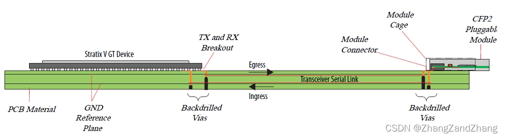
The channel layout on the PCB is optimized in order to meet the strict insertion and return loss masks defined by CEI-28G-VSR.
Refer to the following documents for more information on optimizing your board designs for high speed serial links.
Related Information
• AN529: Via Optimization Techniques for High-Speed Channel Designs
• AN530: Optimizing Impedance Discontinuity Caused by Surface Mount Pads for High-Speed Channel Designs
Stratix V GT Transceiver Channels
Stratix® V GT FPGAs offer four transceiver channels (ATT_TXR[3:0]_P/N and ATT_RXR[3:0]_P/N) that can operate up to 28 Gbps for interfacing with CFP2 or other optical modules.
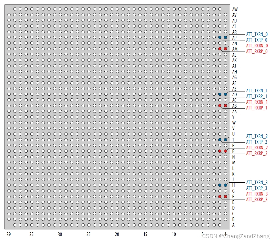
Figure 2: Top View of 28 Gbps Transmitter and Receiver Channel Locations in Stratix V GT FPGAs
CFP2 Host Connector Assembly and Pinout
The CFP2 specification defines the mechanical connector requirements for the 104-pin CFP2 connector. The host connector assembly is composed of a female host connector, and a metal connector cover and cage for retention and electromagnetic shielding of the inserted CFP2 optical module.
Figure 3: CFP2 Host Connector Assembly for a 4x25G/28G Module Interface as Defined by the CFP2 Mechanical Specification

Note: This figure is courtesy of Yamaichi Electronics.
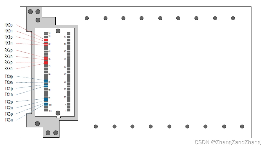
Figure 4: CFP2 Host Connector Pinout for 4x25G/28G Module Interface as Defined by the CFP2 Mechanical Specification
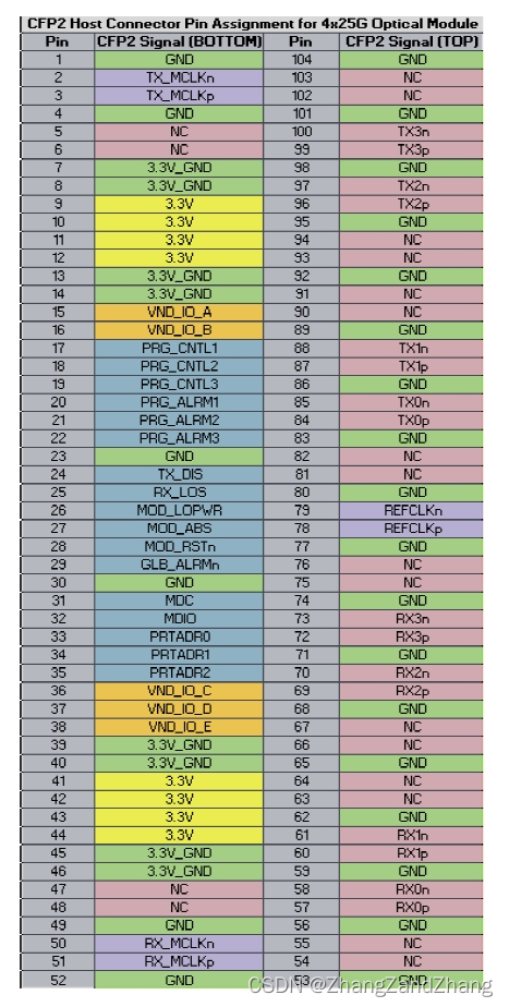
Figure 5: CFP2 Host Connector Layout Footprint
The high-speed transceiver pins are identified in the following figure to show their position within the connector. Blue pins are the TX transceiver channels and red pins are the RX transceiver channels.
Stratix V GT to CFP2 Interface Layout Design
The TX and RX channels are connected directly to the CFP2 connector with approximately 5.5 inches of differential trace routing on the top and bottom layer of the board. DC blocking capacitors are included in the optical module for both the TX and RX traces. Nominal trace impedance is controlled at approximately 100Ω differential and the board material used is Panasonic Megtron-6.
Figure 6: Stratix V GT to CFP2 Interface Layout Design Example
The figure shows an example layout design where the green traces are the TX channels routed on the top layer while the orange traces are the RX channels routed on the bottom layer.
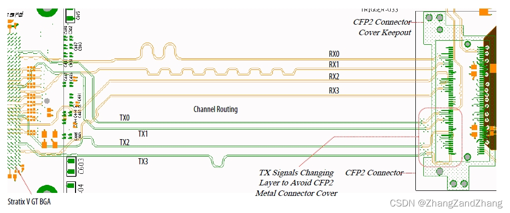
In this example, vias are used for the RX channel breakout at the BGA, and for both the TX and RX channels at the CFP2 connector. To avoid the top layer keep out requirement of the CFP2 metal connector cover assembly, the TX channel routing is switched briefly to the bottom layer and then back to the top layer at the CFP2 connector as illustrated by the circled area in the above figure. Top to bottom routing is used to avoid via stubs.
The BGA pads, signal vias, and CFP2 trace to pad interfaces are large discontinuity sources in the channel. Ansys HFSS (High Frequency Structural Simulator) 3-D field solver simulation is used to optimize the BGA breakout and CFP2 interface design. The trace impedance is kept within ±10% of the nominal 100Ω
Board Stack Up Dimensions
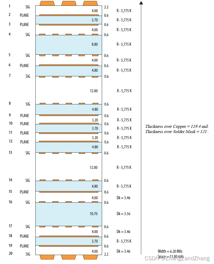
The detailed trace design and board stack up dimensions are shown in the figure below.
Figure 7: Differential Trace Construction and Stack Up Details
BGA Breakout Optimization
BGA breakout optimization targets both the BGA pads and dog bone vias. A cutout is provided in the reference plane under the BGA pad and large oval via anti-pads are used for better BGA pad and via impedance matching.
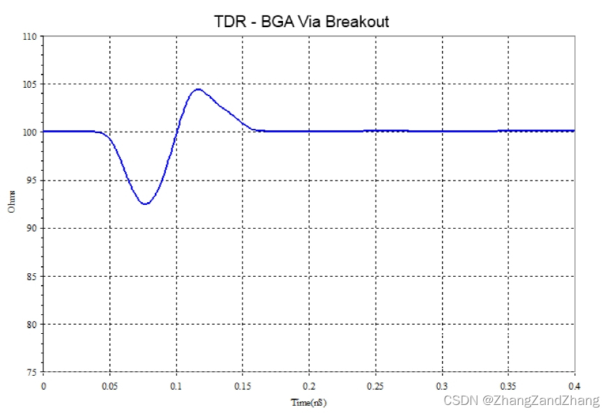
Figure 8: BGA Via Breakout Layout Optimization
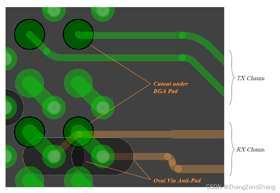
Figure 9: TDR of BGA Via Breakout
HFSS simulation results show that the TDR deviation of the BGA escape is maintained within ±10% of the nominal 100Ω channel target impedance.
CFP2 Interface Optimization
The CFP2 host connector layout optimization reduces the impact of discontinuity at the differential pair to the CFP2 connector interface. A reference plane cutout is provided beneath the connector pads and larger oval anti-pads are used for the signal vias. Four nearby ground return vias are provided to help reduce the connector interface discontinuity.
Figure 10: CFP2 Connector Interface Layout Optimization
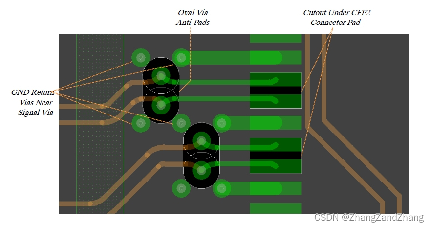
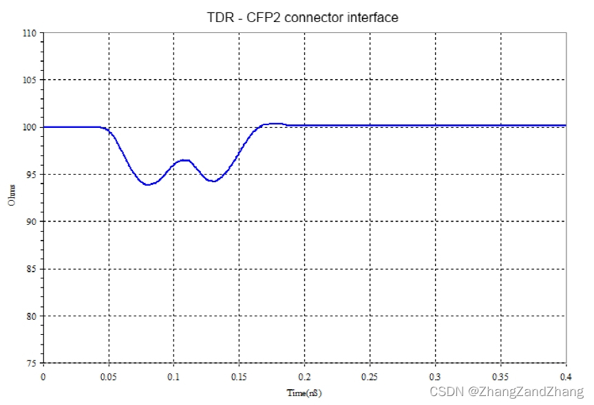
Figure 11: HFSS Simulated TDR of the CFP2 Connector interface
The following figure shows the HFSS simulated TDR results. With the layout optimizations, the TDR deviation due to the discontinuity caused by the via and connector pad is kept within ±10% of the nominal 100Ω target impedance.
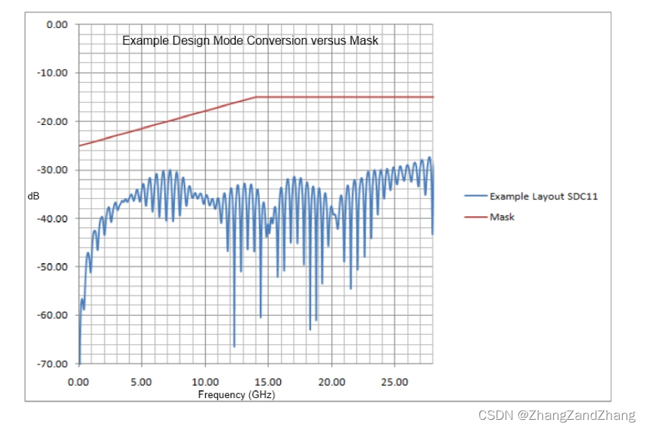
Example Design Channel Performance
The CEI-28G-VSR working clause defines several mask requirements for the channel, including insertion loss, return loss, and differential-to-common mode conversion. Because it is difficult to verify electrical parameters of a full channel in a system, the working clause also defines a Host Compliance Board (HCB) with test points for verifying the host-to-module channel performance at various test points.
Figure 12: Host Compliance Board Measurement Points
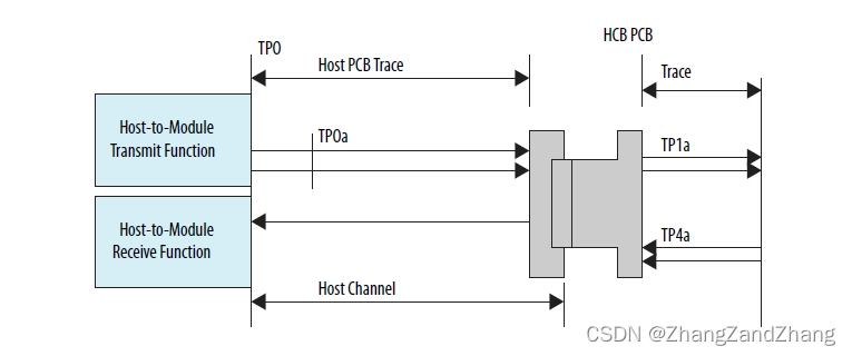
For example, TP1a and TP4a define the measurement points and the associated mask requirements for the host-to-module electrical signal performance for insertion loss, return loss, and differential-to-common mode conversion. For more information about these definitions, refer to the CEI-28G-VSR working clause specification (document number OIF2010.404.08).
Simulation Results for Stratix V GT to CFP2 Connector Layout Design
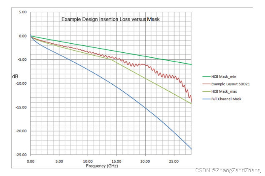
Ansys HFSS (High Frequency Structural Simulator) simulation results for the insertion loss (SDD21), return loss (SDD11) and differential-to-common mode conversion (SDC11) of the channel with the CFP2 connector included are shown in the following figures. The simulation models the HCB for validating the channel layout against the CEI-28G-VSR defined masks.
Figure 13: Insertion Loss versus CEI-28G-VSR Mask Requirements
The SDD21 resides within the HCB minimum and maximum insertion loss masks as defined by the CEI-28G-VSR specification. This insertion loss meets the complete VSR channel (host board + connector + optical module) mask requirement with ample margin to accommodate the additional loss of an inserted CFP2 optical module. Note that the complete channel with the optical module is not simulated.
Similarly, the figures below show that the return loss and differential-to-common mode conversion both meet their respective masks as defined by the CEI-28G-VSR requirement.
Figure 14: Return Loss versus CEI-28G-VSR Mask Requirements
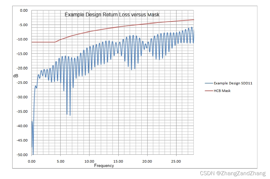
Figure 15: Mode Conversion versus CEI-28G-VSR Mask Requirements