文章目录
- PVT&OCV(local variation)
- Sources of variation
- 1) Etching
- 2) Oxide Thickness
- propagation delay、ld、drain current
- CPPR&CRPR
- setup check
- Hold check
芯片的delay由两部分影响因素构成
- cell delay:library set pvt_corner
- net delay: rc tech file,(RC corner 会受到 Temperature 影响)
- Cadence:icf、captable、qrctechfile
- Synopsys:itf 、Tlu+、nxtgrd
PR工具读入文件MMMC:constrain mode(sdc) + library set pvt corner + rc tech file(rc_corner)
- ocv(芯片上固定pvt的local variation)
PVT&OCV(local variation)
标准单元库(时序库)中的cell delay是在某个固定的PVT(operating condition)下仿真得出的,也就是下图中的Nominal delay。
Nominal delay是在固定PVT下仿真得出的delay,而实际上由于OCV的影响,管子的delay是呈高斯分布或门特卡洛分布,要想保证良率(yield),就必须在timing sign-off时将OCV考虑在内,以保证大部分管子都可以满足时序要求。
对每一代工艺,foundry都会做大量测试,针对每个corner找到一组适合的OCV值,这组值可以保证足够高的良率(yield),而如果进一步加紧这个值,并不会更有效的提高yield。
-
OCV 中的timing derate
-
在SOCV/POCV里的多少sigma(如:3-sigma)的选取也是出于相同的考虑


而实际上在芯片内部由于工艺偏差、电压降、温度变化,cell的delay并不是一个固定值(local variation),而是一个随机值,遵循高斯分布(正态分布),在STA中用OCV(芯片不同位置上PVT分布不同)来模拟这一特征, OCV全称on chip variation,用于描述不同管子间由于工艺偏差、电压降(IR drop)、温度变化(PVT variation)引起的delay变化,也用于描述工艺偏差引起的net厚度宽度的变化从而导致net的电容电阻变化。
提出OCV来模拟(local variation)对芯片 cell delay(timing)的影响
Sources of variation
1) Etching
Look into the below layout of an inverter (which also shows the Width (W) and Length (L) parameters of an inverter)


We use photo-lithography fabrication technique to build the inverters on Silicon wafer, and this is a non-ideal process, where the edges will not exactly be straight lines, but there will be disturbances.
And why so, because the above technique needs photo-masks which are created using etching, which is again non-ideal. Below is how the ideal mask and real mask look like

Now these variations on the sides, is also dependent on what logic cell is present on either sides of this inverter,if its surrounded by chain of inverters on either sides, the variation on the sides will be less as the process parameters to build mask for a chain of similar size inverter, is almost the same.
The inverters on the boundaries will have different and more variations

- 多个cell 挨着,中间的cell process variation 小,边上的cell process variation大 (后端中physical cell endcap/boundary cell 保证
工艺(边界标准单元的物理环境)一致性)

this directly impacts the drain current below, as it is proportional to (W/L) ratio

- Where u is mobility of charge carriers(载流子的迁移速率,温度升高,迁移速率降低)
- Cox(εox/tox) is capacitance per unit area(单位面积氧化层电容。–和Tox成反比)
- W is width of channel,L is channel length(这里指的是gate length/channel length----工艺多少nm指的就是这个)
- Vgs is gate to source voltage,Vth is threshold voltage and Vds is drain to source voltage.
We can observe from drain current equation Id is directly proportional(正比) to (W/L), when we think of a capacitor at the output of an inverter then capacitor charging depends on the amount of current that is flowing it.If drain current changes the amount of time taken by capacitor definitely changes.
-
If drain current (Id) is high then capacitor takes less amount of time to charge and hence delay is minimum.
-
If drain current (Id) is low then capacitor takes huge amount of time to charge and hence delay is maximum.
-
Hence we can say that delay decrease with increase in current and vice versa
2) Oxide Thickness

- if we go by actual oxidation process, its very difficult or almost impossible to achieve the above perfect oxide thickness.
- Below is what you will actually get

So, what’s wrong having above oxide thickness. Again, its the drain current (which is a function of oxide thickness, shown in below image) that will get varied for the complete chain of inverter, especially, the one’s on the sides.(chain of inverter两侧影响最大,endcap 保证stdcell 物理一致性 )

where Cox=εox/tox ,Id is inversely proportional to tox.(thickness of oxide) 、ε--epsilon
If the value of tox changes the value of drain current is also changes.
Now we will see how delay of cell is related to W/L and tox from formula point of view, we know that delay of a cell depends on resistance® and capacitance© and from ohm’s law resistance varies as current changes.
Delay (tpd)=function(R,C)=f(Id)=f(tox,W,L)
propagation delay、ld、drain current
So, overall, its the RC time constant that actually decides the delay of a cell
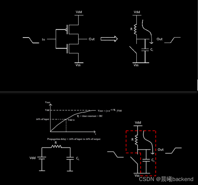
时序库/标准单元库 input/output延迟阈值点、转换率阈值点设置(一般为50%)
##NLDM
input_threshold_pct_fall:50.00
input_threshold_pct_rise:50.00
output_threshold_pct_rise:50.00
output_threshold_pct_fall:50.00

slew_lower_threshold_pct_rise:30.00
slew_upper_threshold_pct_rise:70.00
slew_lower_threshold_pct_fall:30.00
slew_upper_threshold_pct_fall:70.00
slew_derate_from_library:0.5

##标准单元库中的transition time(如10-90)*slew_derate_from_library=实际设定的转换率阈值对应的transition time
With above, we can safely say, the propagation delay tPD is a function of ‘R’
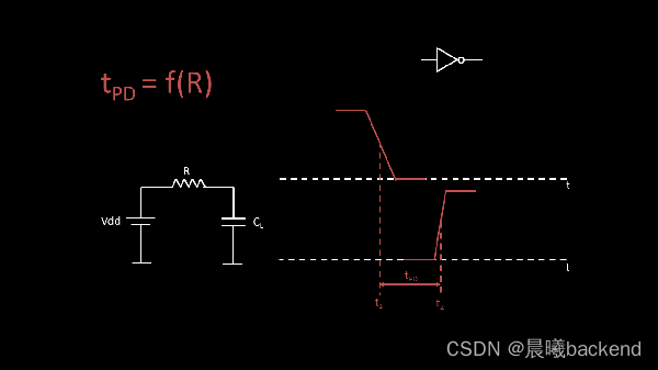
from previous posts, we seen variation in drain current ‘Id’ due to variation in ‘W/L’ and ‘oxide thickness’ variations, and above we see, how propagation delay is function of ‘R’.
that drain current ‘Id’ strongly depends on ‘R’, then I can directly relate (W/L) and oxide thickness variation to ‘R’, and below images will exactly do that

Hence, every inverter in the below chain, will have delay which is different
- middle stdcell process variation 小
- side stdcell process variation 大

可以用高斯分布曲线表征

- normal delay 的 cell占多数
- increase delay 和 decrease delay 占少数
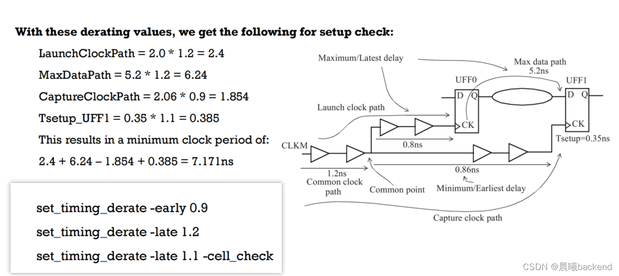
For setup calculation, the launch clock will have OCV of +8% and capture clock path will have OCV of -9%. That means, if the original clock cell delay is ‘x’ in launch clock, with OCV into account, the same clock cell delay will be (‘x’ + 0.08x). This calculation in setup takes into account the On-Chip Variation
实际setup已经是worst_corner了(够慢了),hold已经是best_corner (够快了)
- setup 的 capture path derate -9%
- hold的 capture path derate +8%
CPPR&CRPR
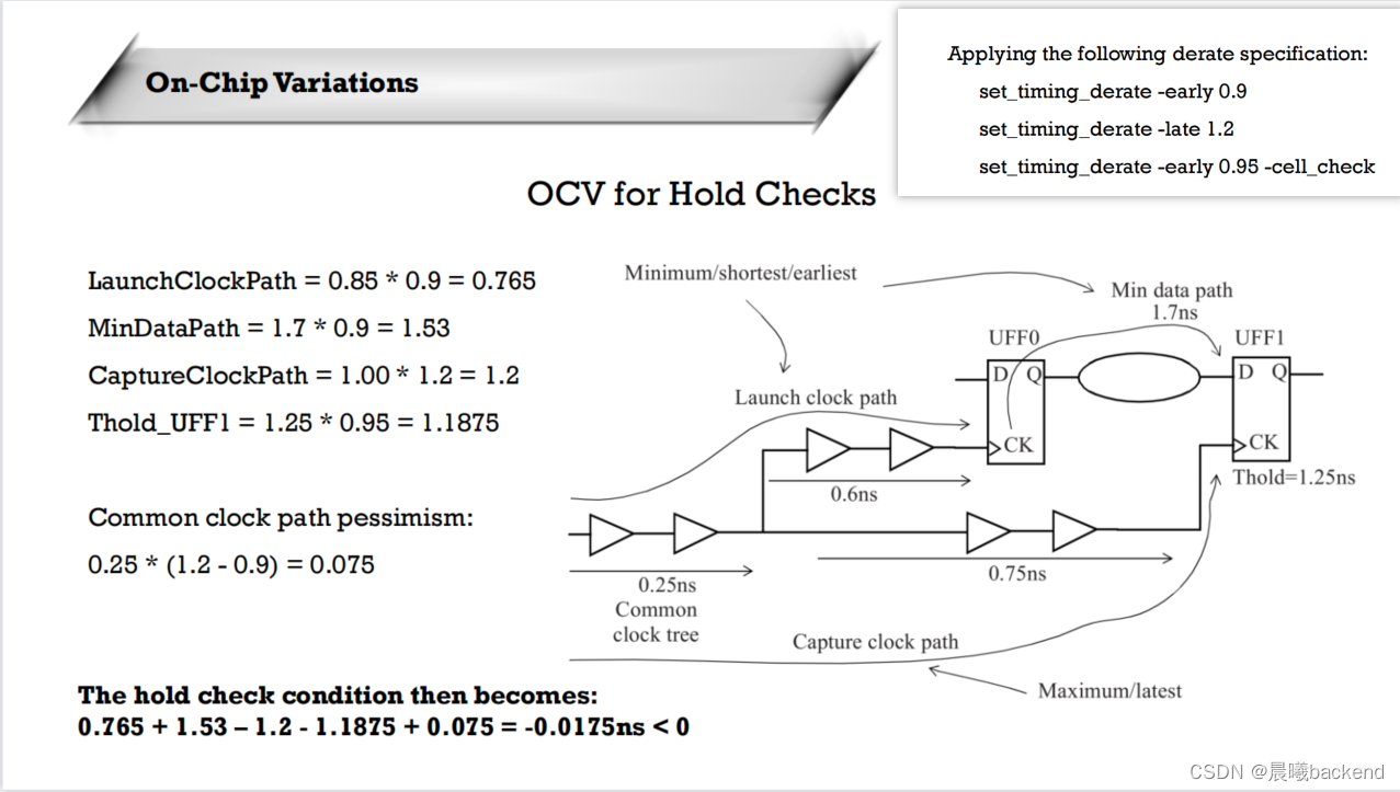
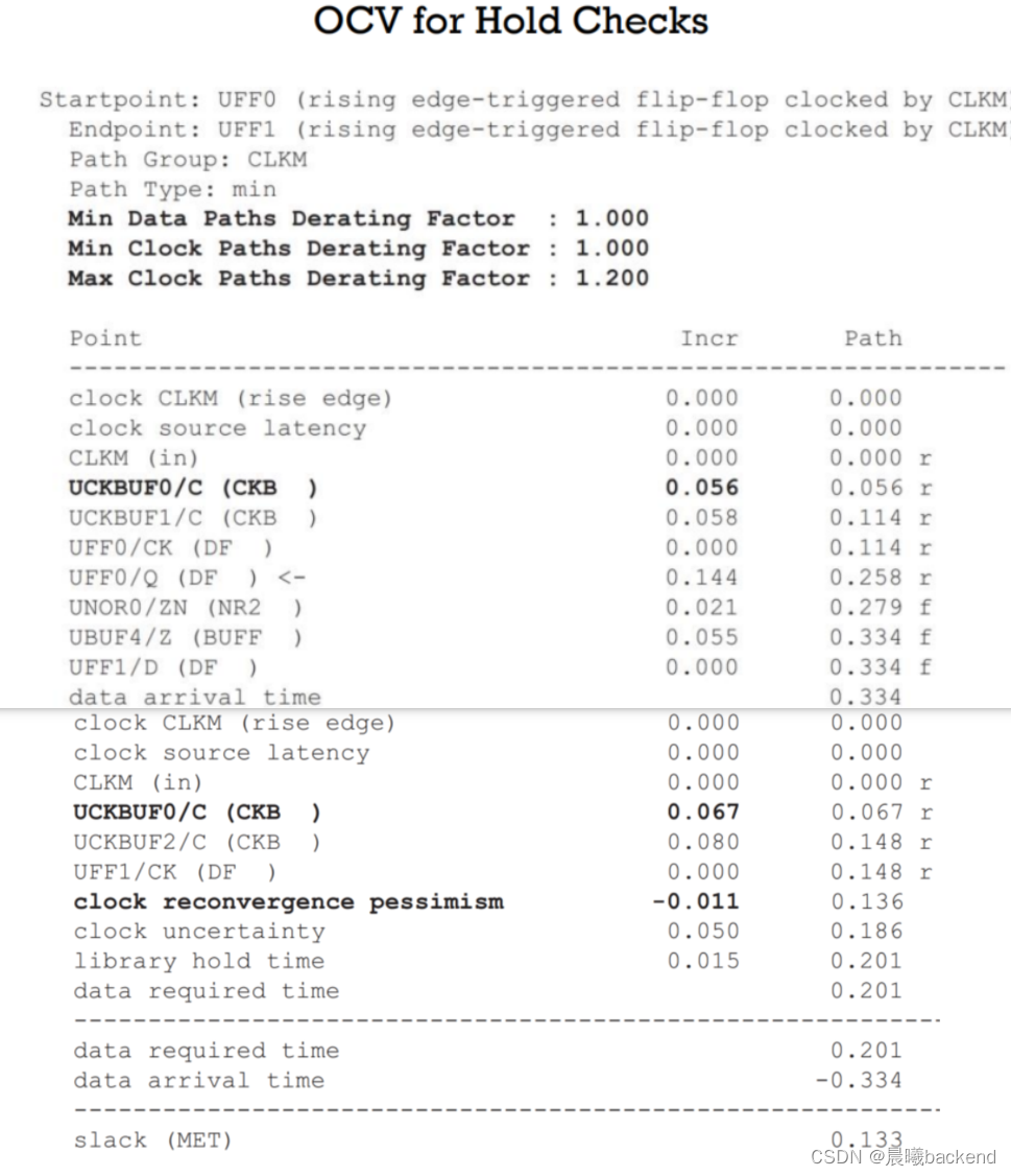
- Common Path Pessimism Removal/Clock Recovergence Pessimism Removal
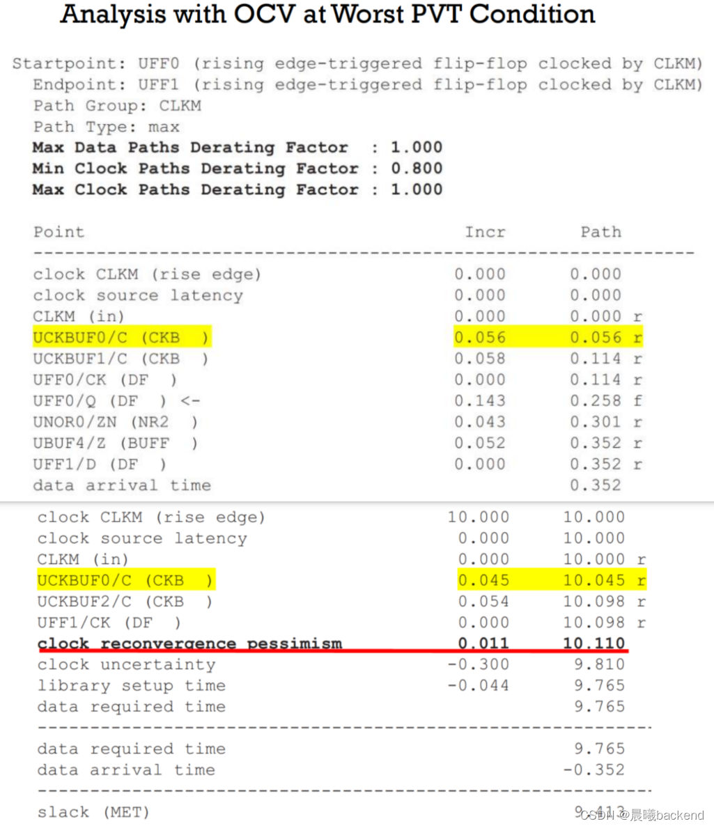
launch clock path和capture clock path 存在common path,这条common path 用early derate算了一遍又用late derate算了一遍,相当于算了两遍,因此要去除多算的这部分
setup check
-
对于setup check ,captute path 设置了 early derate,CPPR在report中的require time中加上即可
-
T = Tcq+Tcomb+Tsu - Tskew(capture clock path - launch clock path)
Hold check
- Tcq+Tcomb - Thold - Tskew(capture clock path - launch clock path) > 0
- CPPR 在require time中减去
