文章目录
- 《专用集成电路设计实用教程》
- 集成电路系统的组成
- 集成电路的设计流程
- 综合=转化+逻辑优化+映射
- 同步电路和异步电路
- 亚稳态
- 单时钟同步设计的时序约束
- 目标库和初始环境设置
- DC如何计算每个逻辑单元的延迟(Cell Delay)?
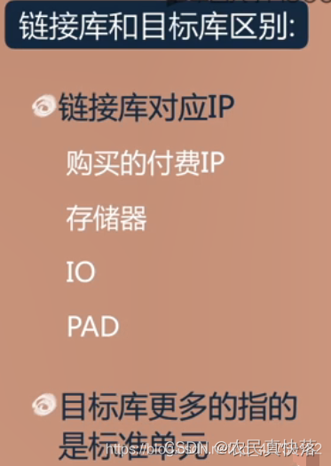
- target library
- link library
- 《高级ASIC芯片综合》
- 《数字集成电路物理设计》
- 《VLSI Circuit Design Methodology Demystified》
- 69. WHAT IS FLOORPLANNING?
- 个人总结
打算后面将IC设计流程方面的书籍笔记记在这里,近期每天持续更新(
除非导师换方向)
《专用集成电路设计实用教程》
集成电路系统的组成
-
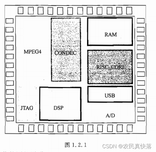
数字电路模块:RISC_CORE
大部分数字电路使用同一个时钟源,经过时钟产生电路,协同各部分运行。即同步电路。
数字电路大致可以分为数据通路和控制通路。数据通路指进行加减乘除的运算器,控制通路是控制数据流通和信号开关等的逻辑电路。 -
模拟电路模块:A/D
模拟电路相关的有模数转换器ADC,数模转换器DAC,
可编程增益放大器PGA,通过数字电路来控制模拟增益
锁相环PLL,用于产生高频时钟和进行时钟信号的相位校正 -
IP核模块:MPEG4、DSP、CONDEC、USB
IP核的出现是IC产业分工的结果,使得一些公司写IP,一些公司复用IP,从而IP用的放心,也开发的更快。
USB是IP核,也是输入输出设备。 -
内存模块:RAM
内存占据了大部分芯片面积,在低功耗设计中要注意内存功耗在芯片功耗中的比例。 -
输入输出PAD
这里的PAD就是端口的意思,USB接口就是一种I/O PAD。
由于I/O PAD是直接与外部世界相连接的特殊单元,因此要考虑外部电路的寄生参数影响、静电保护、封装要求、电压转换、过压保护、信号完整等。
I/O PAD分为:输入PAD、输出PAD、双向PAD。
个人总结:
感觉I/O PAD是比较容易被忽略的学习点,在实际工作中可能很重要,因为在招聘中经常看到要懂SPI、I2C、UART,还有高速接口设计,DDR,PCIe,Ethernet,Serdes。
- 边界扫描模块:JTAG
相比于传统万用表和示波器测试芯片的“探针”类方法,JTAG是在芯片的边界加上一些寄存器,可以实现对芯片输入输出信号的观察和控制,提供一种不影响芯片运行的调试芯片的方法。
个人总结:
感觉就是跟写程序debug一样的功能
- 互联线
芯片的模块之间需要互连线来交换信息,互连线包括信号线和电源线,其本质是金属,具有电容、电阻和电感效应,这些称为寄生效应,这些寄生效应会产生连线信号的延迟!
在超深亚微米设计(180nm以下)中,连线延迟已经和逻辑门的延迟相当,因此在计算时序路径延迟时,不可以再使用线负载模型估算连线的延迟。为解决该问题,Synopsys推出物理综合工具和拓扑综合技术,在书第七章介绍。
个人总结:
dc综合时没考虑互连线的寄生效应(或者只是考虑了线负载模型,并不全面),互连线的寄生效应要在后仿时考虑进去,涉及到StarRC和PT工具。
关于负载与RC,这个视频里有讲。
RC负载与延迟
集成电路的设计流程
其实dc和icc似乎并不是割裂的工具,他们采用的数据格式是互通的,突然发现这一点。
将RTL源代码输入到DC,给设计加约束,进行逻辑综合,得到门级网表,该网表可以以ddc存放,也可以用Milkyway存储。2~9章讲了很多dc的内容。
然后是布图规划(包括供电规划)、布局、时钟树综合、布线,StarRC提取寄生参数,然后输入到PT中进行时序和功耗分析。PrimeTime
( PX是一个可以同时进行时序和功耗分析的签核工具)
综合=转化+逻辑优化+映射
- 转化: 先将RTL源代码转化为通用的布尔等式——GTECH格式;
- 逻辑优化:然后按照设计的约束对电路进行逻辑综合和优化,使得电路能满足设计的目标或约束;
- 映射:最后使用目标工艺库的逻辑单元映射成门级网表。综合的结果包括了电路的时序和面积。
个人总结:
先通过read命令将RTL代码转化为GTECH格式,实际上就是布尔代数的等式,然后在用compile命令时会进行逻辑综合、优化、映射。
同步电路和异步电路
同步电路指电路中所有时钟来自同一个时钟源,
异步电路指电路中的时钟来自不同的时钟源。
个人总结:
如果来自同一个时钟源,例如300HZ,即使经过3分频,6分频分为100HZ和50HZ两个时钟,相位也必然一致。
如果来自不同的时钟源,相位就不一定一致了。
亚稳态
书中解释的不是特别清晰,我又ChatGPT问了以下,懂了:
Setup Time指的是输入信号在时钟上升沿之前必须保持稳定的最小时间间隔。如果输入信号在时钟上升沿之前没有保持足够长的稳定时间,那么电路输出可能无法正确响应。
Hold Time指的是在时钟上升沿之后,输入信号必须保持稳定的最小时间间隔。如果输入信号在时钟上升沿之后没有保持足够长的稳定时间,那么电路输出也可能无法正确响应。
举个例子来说,假设有一个触发器电路,其时钟信号为CLK,数据输入信号为D。该电路的Setup Time为5纳秒,Hold Time为3纳秒。如果输入信号D在CLK的上升沿之前保持稳定状态至少5纳秒,并且在CLK的上升沿之后保持稳定状态至少3纳秒,那么电路输出会正确响应。否则,输出可能会出现错误的值或亚稳态行为。

个人总结:
一个D触发器,在时钟上升沿时,D的值要传递给Q,自然就要在时钟上升沿对D进行采样。为了保证采样的值是对的,那就不允许上升沿前后D有变化,上升沿之前这个禁止变化的时间是setup time,上升沿之后的这个时间是hold time。
下降沿也同理。
单时钟同步设计的时序约束
D数据在哪?看的不太懂。
个人总结:
大意就是从一个io口到另一个io口之间花的时间不能太长,否则等你信号过来了,我这个周期的采样早结束了,功能也就不能在一个周期实现了。
这本书是在Synopsys公司的逻辑综合培训资料基础上编写而成,讲了不少dc的细节,估计就是参考了User Guide的文档。
目标库和初始环境设置
DC如何计算每个逻辑单元的延迟(Cell Delay)?
单位的时延与输入的逻辑转换时间(Input Transition Time)和输出的负载(Output Load)有关,根据这两个数据,可以在库中的查找表(Look up table)中查出单元的延迟。
延时的计算由线性方法和非线性方法,目前主要用非线性方法。这篇文章写的很清楚:
Synopsys逻辑综合及DesignCompiler的使用
target library
DC中,target_library是保留变量,设置这个变量以指向厂商提供的综合库文件。
link library
set link_library “* my_tech.db”
星号表示DC先搜寻其内存里已有的库;一般放在综合库之前。

《高级ASIC芯片综合》
下载了pdf,等我看了再总结
《数字集成电路物理设计》
据说是国内第一部系统介绍VLSI的书,讲得很好(一点看不懂 )
《VLSI Circuit Design Methodology Demystified》
69. WHAT IS FLOORPLANNING?
Floorplanning is the first major step in physical design. The key tasks in this step include analyzing the die size, selecting the package, placing the I/Os, placing the macro cells (e.g., memory cells, analog cells, and specialfunction cells), planning the distribution of power and the clocks, and partitioning the hierarchy.
Die size estimation often starts from the gate count of the netlist (available from the logic synthesis process) plus the physical size of the I/Os and macros. A design can be characterized as I/O limited, core limited, block limited, or package limited. The die size of an I/O-limited design is determined by its number of I/Os. The full placement of the prime input and output cells will dominate the physical size of this chip. On the other hand, in a core-limited design, the size of the chip is governed by the core area or the number of standard and macro cells used. In this case, there is probably room to compensate for a few more I/O signals without increasing the chip size. In a block-limited design, there usually are a significant number of large blocks, or subchips, and the chip size is dominated by the sizes of
those blocks. For a package-limited design, the chip size is driven by the available package. Package selection is another major issue that affects the physical design.The selection is based on a number of factors, such as the number of I/Os, the die size, the chip power consumption, and the price. To compensate for the slightly different die sizes, there may be several lead frames available for the same package.
After the package has been fixed, the next crucial step is to arrange the prime input and output cells. I/O configuration has a direct impact on the quality of physical layout since the placement of the rest of the standard cells and macros depend on the I/O locations. The routability of the chip is also closely tied to the I/O configuration. Among many issues, one of the key issues in I/O configuration is the placement of the power and ground pins. These pins, which could amount to up to one-third or more of the total number of I/Os, are placed carefully to reduce or eliminate any IR drop or EM problem. Additionally, for complicated SoC chips with many analog macros, there are various special power supplies other than VDD (for core) and VDDS (for I/O). Many of them have to be separated from the main
VDD/VSS busses for noise immunization. In such cases, chip I/O planning becomes an even tougher challenge. Macros such as memories and analog cells are often placed manually by designers based on I/O configuration. Designers must reduce overall routing
congestion so as not to create major hurdles for meeting the chip timing target. The placement of those special cells has a great impact on the overall chip placement quality and, consequently, can significantly affect the chip’s overall routability. In most cases, it takes several iterations to find good locations for those macros.
In a VLSI chip, every single transistor needs power to perform. The required power is delivered to the transistors through a power distribution network. This network is called the power plan, or power structure, of the chip. This power network must deliver the appropriate voltage level to the transistors within the chip for their entire lifetime. The two most critical problems associated with a power network are the IR drop and EM. When the effective resistance of the power network is beyond a certain level (such as that caused by narrow metal lines), the voltage drop (I · R) from the source to the destination could be higher than what is tolerable. In such cases, the destination transistors might not function correctly. This is the IR drop problem.
In addition to IR drop, the current flowing through the metal line is constantly pushing and moving the metal atoms. The magnitude of this action is proportional to the current density. After a lengthy period of such action, the
metal structure can become damaged, and opens or shorts may result. This
is the electromigration (EM) problem. The EM problem will negatively affect a product’s life span.
In today’s chip operation, almost every action inside the chip is operating
on some clock signal. All of the storage elements (flip-flops, latches, and
memories) are switched on and off by various clocks. Undoubtedly, the entire chip operation is coordinated by clocks (see Chapter 3, Question 25).
Delivering the clock signals reliably to the needed elements is a necessity in
physical design. This task is commonly called clock tree synthesis (CTS).
The two basic concerns in CTS are clock skew and clock tree insertion delay. CTS is a very complicated issue since there are many clock domains in
a typical SoC design, and each domain has its own requirement. Sometimes,
the clock trees between different clock domains must be balanced as well.
Furthermore, in the test mode, the cells in various clock domains must be
working at the same testing clock speed. This puts additional constraints on
the clock structure.
Another influential issue in floorplanning is hierarchy partition. In some
designs, especially large designs, size constraints prevents the entire design
from being handled at once by the tools. In such situations, the divide-andconquer strategy is adopted. A good partition can turn an otherwise unachievable design into a doable one. It can also help speed up the implementation process significantly by enabling parallelism. However, the trade-off
is the efficiency of the area and timing. In other words, hierarchical design
is not as efficient as flat design in terms of area and timing since the place
and route tool cannot see the whole picture at once and consequently cannot
perform the optimization as one whole piece.
Figure 4.27 is one floorplan example of a real chip. In this chip, there are
almost 400 I/Os, which are located on the chip periphery. About one-third
of them are power and ground pins. There are five PLLs, one DLL (delaylocked loop), one high-speed DAC, one large, hard macro on-chip proces-sor, and more than 80 SRAM memories in this mixed-signal SoC chip. The
central area is reserved for standard cells. As apparent in the figure, there
are two levels of physical hierarchies: the top level and the standard cell and
macro level. As addressed in Question 68, the place and route tool cannot
handle the physical hierarchy very efficiently. Having more than two levels
of physical hierarchies degrades the quality of the implementation significantly.
The five on-chip PLLs are placed carefully with plenty of space in between. This configuration can effectively reduce interference among the
PLLs. The large hard macro is placed in the lower right-hand corner to minimize the impact on the chip’s overall routability. The analog DAC is also
located in one corner to achieve maximum isolation from the rest of the digital blocks. All of the analog blocks (DAC, PLLs, and DLL) have guard
rings embedded in the cell-level layout to minimize noise coupling from the
digital circuitry. Moreover, to further trim noise coupling, each analog cell
has its own ground, which is not metal-connected to the chip’s main digital
ground (substrate).
This floorplan is the starting point for the subsequent place and route
steps
个人总结
感觉这一段写的比较好,明天总结一下。

