本次使用CubeMx配置FSMC驱动SRAM,XM8A51216 IS62WV51216
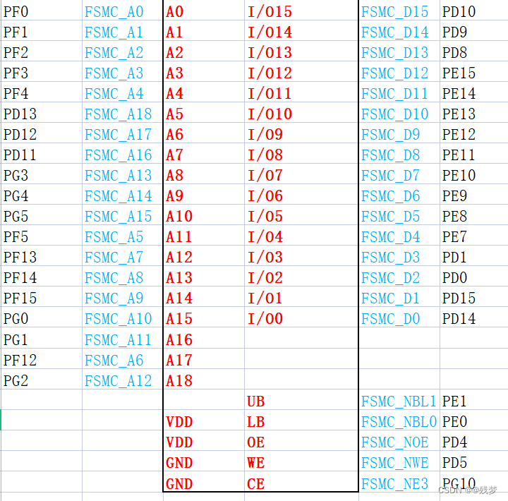
原理图:

注意:FSMC_A0必须对应外部设备A0引脚
一、FSMC和FMC区别
FSMC:灵活的静态存储控制器
FMC:灵活存储控制器
区别:FSMC只能驱动静态存储控制器(如:SRAM),FMC只能驱动动态存储控制器(如:SDRAM)
注意:FMC是不能驱动SRAM的,同理FSMC不能驱动SDRAM
二、FSMC知识点
1、地址性问题
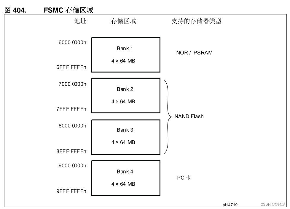
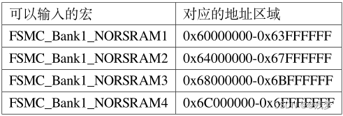
驱动SRAM需使用Bank1区域


原理图中可以看出,我们选用的是FSMC_NE3;所以无论地址线FSMC_A1->FSMCA18怎么错位接,地址都是程序中映射SRAM地址时自然而然为0x6800 0000;因为地址具有唯一性,能够和内存地址一一对应;但是FSMC_A0必须对应外部设备A0引脚;
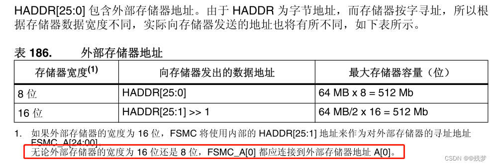
注意:在使用LCD时,设备是没有地址线(A0-A18)的,但有RS(数据|命令)线,此时我们要特别注意 HADDR[25:0]的对应关系:
当 Bank1 接的是 16 位宽度存储器的时候:HADDR[25:1]→ FSMC_A[24:0]。
当 Bank1 接的是 8 位宽度存储器的时候:HADDR[25:0]→ FSMC_A[25:0]。
解释:RS信号线:0–命令,1–数据
比如说正点原子探索者的LCD接线,RS接在FSMC_A6上;
如果要对LCD进行写命令,则应FSMC_A6 = 0;写数据则FSMC_A6 = 1;
LCD使用的是 16 位数据宽度,所以 HADDR[0]并没有用到,只有 HADDR[25:1]是有效的,对应关系变为:HADDR[25:1]→FSMC_A[24:0],相当于右移了一位;
写地址0x40;(0100 0000),此时bit6为1的,但是右移1位
写地址为0x20;(0010 0000),此时bit6为0和引脚FSMC_A6对应连接,导致LCD写命令
那LCD写完命令马上写数据咋办呢,地址指针由结构体可以看出,LCD_REG写命令后,LCD_RAM部分写数据,结构体地址会加2(u16为2字节)
LCD定义结构体
typedef struct
{
vu16 LCD_REG;
vu16 LCD_RAM;
} LCD_TypeDef;
但是想想0x40 + 2 = 0x42,即使右移1位后,bit6任然是0,所以无法实现写命令后接着写数据
所以应想想写数据(100 0000),让bit6为1,那么还原右移之前的数据为0x80 => 1000 0000;
则写命令地址 = 0x80 - 2 = 0x7E
0x7E => 0111 1110;右移1位变为0011 0000,此时bit6为0,所以FSMC_A6为0,RS写命令
所以如下所示:

0x6C00 0000是NE4地址

2、时序性问题
FSMC 外设支持输出多种不同的时序以便于控制不同的存储器,它具有 ABCD 四种模式,下面仅针对控制 SRAM 使用的模式 A 进行讲解

Byte enable
这个功能是使能控制FSMC_NB[1:0]
UB 接 FSMC_NBL1 //高字节
LB 接 FSMC_NBL0 //底字节
Address setup time in HCLK clock cycles:Address setup time in HCLK clock cycles must be between 0 and 15.
Data setup time in HCLK clock cycles:Data setup time in HCLK clock cycles must be between 1 and 255.
Bus turn around time in HCLK clock cycles:Bus turn around time in HCLK clock cycles must be between 0 and 15.
**Address setup time in HCLK clock cycles:**地址建立时间(ADDSET)
**Data setup time in HCLK clock cycles:**数据建立时间(DATAST)
**Bus turn around time in HCLK clock cycles:**总线周转阶段的持续时间;总线周转是每次操作的间隔时间


此处时序计算可以看看野火方法


二、CubeMx配置FSMC驱动SRAM 芯片:IS62WV51216
芯片接线图
1、CubeMx配置


生成代码
2、SRAM测试

main.h文件添加
#include "stdio.h"
stm32f4xx_it.c文件添加硬件中断提示
/**
  * @brief This function handles Hard fault interrupt.
  */
void HardFault_Handler(void)
{
  /* USER CODE BEGIN HardFault_IRQn 0 */
  printf("void HardFault_Handler(void)\r\n");
  /* USER CODE END HardFault_IRQn 0 */
  while (1)
  {
    /* USER CODE BEGIN W1_HardFault_IRQn 0 */
    /* USER CODE END W1_HardFault_IRQn 0 */
  }
}
main.c添加SRAM数据读写测试函数和打印函数
主函数调用测试TestSRAM();
/* USER CODE BEGIN Header */
/**
******************************************************************************
* @file : main.c
* @brief : Main program body
******************************************************************************
* @attention
*
* <h2><center>© Copyright (c) 2023 STMicroelectronics.
* All rights reserved.</center></h2>
*
* This software component is licensed by ST under BSD 3-Clause license,
* the "License"; You may not use this file except in compliance with the
* License. You may obtain a copy of the License at:
* opensource.org/licenses/BSD-3-Clause
*
******************************************************************************
*/
/* USER CODE END Header */
/* Includes ------------------------------------------------------------------*/
#include "main.h"
#include "usart.h"
#include "gpio.h"
#include "fsmc.h"
/* Private includes ----------------------------------------------------------*/
/* USER CODE BEGIN Includes */
/* USER CODE END Includes */
/* Private typedef -----------------------------------------------------------*/
/* USER CODE BEGIN PTD */
/* USER CODE END PTD */
/* Private define ------------------------------------------------------------*/
/* USER CODE BEGIN PD */
/* USER CODE END PD */
/* Private macro -------------------------------------------------------------*/
/* USER CODE BEGIN PM */
/* USER CODE END PM */
/* Private variables ---------------------------------------------------------*/
/* USER CODE BEGIN PV */
/* USER CODE END PV */
/* Private function prototypes -----------------------------------------------*/
void SystemClock_Config(void);
/* USER CODE BEGIN PFP */
/* USER CODE END PFP */
/* Private user code ---------------------------------------------------------*/
/* USER CODE BEGIN 0 */
/*SRAM 起始地址 存储空间 3 的起始地址 */
#define Bank1_SRAM3_ADDR ((uint32_t)0x68000000)
uint8_t testValue __attribute__((at(Bank1_SRAM3_ADDR)));
void TestSRAM(void)
{
uint32_t temp = 0;
printf("\r\n指针方式访问 SRAM\r\n");
/* 向 SRAM 写入 8 位数据 */
*( uint8_t*) (Bank1_SRAM3_ADDR ) = (uint8_t)0xAA;
printf("\r\n指针访问 SRAM,写入数据 0xAA \r\n");
/* 从 SRAM 读取数据 */
temp = *( uint8_t*) (Bank1_SRAM3_ADDR );
printf("读取数据:0x%X \r\n",temp);
/* 写 / 读 16 位数据 */
*( uint16_t*) (Bank1_SRAM3_ADDR+10 ) = (uint16_t)0xBBBB;
printf("指针访问 SRAM,写入数据 0xBBBB \r\n");
temp = *( uint16_t*) (Bank1_SRAM3_ADDR+10 );
printf("读取数据:0x%X \r\n",temp);
/* 写 / 读 32 位数据 */
*( uint32_t*) (Bank1_SRAM3_ADDR+20 ) = (uint32_t)0xCCCCCCCC;
printf("指针访问 SRAM,写入数据 0xCCCCCCCC \r\n");
temp = *( uint32_t*) (Bank1_SRAM3_ADDR+20 );
printf("读取数据:0x%X \r\n",temp);
/* 绝对定位方式访问 SRAM, 这种方式必须定义成全局变量 */
testValue = 0xDD;
printf("\r\n绝对定位访问 SRAM,写入数据 0xDD, 读出数据 0x%X, 变量地址为%X\r\n", testValue,(uint32_t )&testValue);
}
int fputc(int ch,FILE *f)
{
uint8_t data = ch;
HAL_UART_Transmit(&huart1,&data,1,1);
return(ch);
}
/* USER CODE END 0 */
/**
* @brief The application entry point.
* @retval int
*/
int main(void)
{
/* USER CODE BEGIN 1 */
/* USER CODE END 1 */
/* MCU Configuration--------------------------------------------------------*/
/* Reset of all peripherals, Initializes the Flash interface and the Systick. */
HAL_Init();
/* USER CODE BEGIN Init */
/* USER CODE END Init */
/* Configure the system clock */
SystemClock_Config();
/* USER CODE BEGIN SysInit */
HAL_Delay(3000);
/* USER CODE END SysInit */
/* Initialize all configured peripherals */
MX_GPIO_Init();
MX_FSMC_Init();
MX_USART1_UART_Init();
/* USER CODE BEGIN 2 */
TestSRAM();
/* USER CODE END 2 */
/* Infinite loop */
/* USER CODE BEGIN WHILE */
while (1)
{
/* USER CODE END WHILE */
/* USER CODE BEGIN 3 */
}
/* USER CODE END 3 */
}
/**
* @brief System Clock Configuration
* @retval None
*/
void SystemClock_Config(void)
{
RCC_OscInitTypeDef RCC_OscInitStruct = {0};
RCC_ClkInitTypeDef RCC_ClkInitStruct = {0};
/** Configure the main internal regulator output voltage
*/
__HAL_RCC_PWR_CLK_ENABLE();
__HAL_PWR_VOLTAGESCALING_CONFIG(PWR_REGULATOR_VOLTAGE_SCALE1);
/** Initializes the RCC Oscillators according to the specified parameters
* in the RCC_OscInitTypeDef structure.
*/
RCC_OscInitStruct.OscillatorType = RCC_OSCILLATORTYPE_HSE;
RCC_OscInitStruct.HSEState = RCC_HSE_ON;
RCC_OscInitStruct.PLL.PLLState = RCC_PLL_ON;
RCC_OscInitStruct.PLL.PLLSource = RCC_PLLSOURCE_HSE;
RCC_OscInitStruct.PLL.PLLM = 4;
RCC_OscInitStruct.PLL.PLLN = 168;
RCC_OscInitStruct.PLL.PLLP = RCC_PLLP_DIV2;
RCC_OscInitStruct.PLL.PLLQ = 4;
if (HAL_RCC_OscConfig(&RCC_OscInitStruct) != HAL_OK)
{
Error_Handler();
}
/** Initializes the CPU, AHB and APB buses clocks
*/
RCC_ClkInitStruct.ClockType = RCC_CLOCKTYPE_HCLK|RCC_CLOCKTYPE_SYSCLK
|RCC_CLOCKTYPE_PCLK1|RCC_CLOCKTYPE_PCLK2;
RCC_ClkInitStruct.SYSCLKSource = RCC_SYSCLKSOURCE_PLLCLK;
RCC_ClkInitStruct.AHBCLKDivider = RCC_SYSCLK_DIV1;
RCC_ClkInitStruct.APB1CLKDivider = RCC_HCLK_DIV4;
RCC_ClkInitStruct.APB2CLKDivider = RCC_HCLK_DIV2;
if (HAL_RCC_ClockConfig(&RCC_ClkInitStruct, FLASH_LATENCY_5) != HAL_OK)
{
Error_Handler();
}
}
/* USER CODE BEGIN 4 */
/* USER CODE END 4 */
/**
* @brief This function is executed in case of error occurrence.
* @retval None
*/
void Error_Handler(void)
{
/* USER CODE BEGIN Error_Handler_Debug */
/* User can add his own implementation to report the HAL error return state */
__disable_irq();
while (1)
{
}
/* USER CODE END Error_Handler_Debug */
}
#ifdef USE_FULL_ASSERT
/**
* @brief Reports the name of the source file and the source line number
* where the assert_param error has occurred.
* @param file: pointer to the source file name
* @param line: assert_param error line source number
* @retval None
*/
void assert_failed(uint8_t *file, uint32_t line)
{
/* USER CODE BEGIN 6 */
/* User can add his own implementation to report the file name and line number,
ex: printf("Wrong parameters value: file %s on line %d\r\n", file, line) */
/* USER CODE END 6 */
}
#endif /* USE_FULL_ASSERT */
/************************ (C) COPYRIGHT STMicroelectronics *****END OF FILE****/

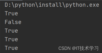
说明SRAM已经正常使用
那不能用的时候会是什么现象呢?
不妨关闭写使能,你会发现系统会在调用SRAM测试函数时,操作指针导致进入硬错误中断
3、完整工程
链接:https://pan.baidu.com/s/18XYVshKugecpefd5L0CeWg
提取码:wcnn
三、代码笔记
使用HAL库前先看下stm32f4xx_hal_sram.c描述的使用方法:How to use this driver
这个驱动程序是一个通用的分层驱动程序,它包含一组用于控制SRAM内存。它使用FMC层函数进行接口使用SRAM设备。按照以下顺序将FMC/FSMC配置为接口SRAM/PSRAM存储器:
(1)定义SRAM_HandleTypeDef句柄变量,赋值结构体
(2)定义FMC_NORSRAM_TimingTypeDef句柄变量,赋值结构体,时序控制
(3)通过调用HAL_SRAM_Init()函数初始化SRAM控制器:
A、这个函数会调用HAL_SRAM_MspInit()函数配置MSP硬件层,
B、配置FSMC外设时钟:__HAL_RCC_FSMC_CLK_ENABLE();
C、引脚配置
然后就可以进行读写操作了
HAL_StatusTypeDef HAL_SRAM_Read_8b(SRAM_HandleTypeDef *hsram, uint32_t *pAddress, uint8_t *pDstBuffer, uint32_t BufferSize);
HAL_StatusTypeDef HAL_SRAM_Write_8b(SRAM_HandleTypeDef *hsram, uint32_t *pAddress, uint8_t *pSrcBuffer, uint32_t BufferSize);
HAL_StatusTypeDef HAL_SRAM_Read_16b(SRAM_HandleTypeDef *hsram, uint32_t *pAddress, uint16_t *pDstBuffer, uint32_t BufferSize);
HAL_StatusTypeDef HAL_SRAM_Write_16b(SRAM_HandleTypeDef *hsram, uint32_t *pAddress, uint16_t *pSrcBuffer, uint32_t BufferSize);
HAL_StatusTypeDef HAL_SRAM_Read_32b(SRAM_HandleTypeDef *hsram, uint32_t *pAddress, uint32_t *pDstBuffer, uint32_t BufferSize);
HAL_StatusTypeDef HAL_SRAM_Write_32b(SRAM_HandleTypeDef *hsram, uint32_t *pAddress, uint32_t *pSrcBuffer, uint32_t BufferSize);
HAL_StatusTypeDef HAL_SRAM_Read_DMA(SRAM_HandleTypeDef *hsram, uint32_t *pAddress, uint32_t *pDstBuffer, uint32_t BufferSize);
HAL_StatusTypeDef HAL_SRAM_Write_DMA(SRAM_HandleTypeDef *hsram, uint32_t *pAddress, uint32_t *pSrcBuffer, uint32_t BufferSize);

/* SRAM Control functions  ******************************************************/
HAL_StatusTypeDef HAL_SRAM_WriteOperation_Enable(SRAM_HandleTypeDef *hsram);
HAL_StatusTypeDef HAL_SRAM_WriteOperation_Disable(SRAM_HandleTypeDef *hsram);
先来看看FSMC的SRAM句柄:SRAM_HandleTypeDef
typedef struct
#endif /* USE_HAL_SRAM_REGISTER_CALLBACKS  */
{
  FMC_NORSRAM_TypeDef           *Instance;  /*!< Register base address                        */

  FMC_NORSRAM_EXTENDED_TypeDef  *Extended;  /*!< Extended mode register base address          */

  FMC_NORSRAM_InitTypeDef       Init;       /*!< SRAM device control configuration parameters */

  HAL_LockTypeDef               Lock;       /*!< SRAM locking object                          */

  __IO HAL_SRAM_StateTypeDef    State;      /*!< SRAM device access state                     */

  DMA_HandleTypeDef             *hdma;      /*!< Pointer DMA handler                          */

#if (USE_HAL_SRAM_REGISTER_CALLBACKS == 1)
  void  (* MspInitCallback)        ( struct __SRAM_HandleTypeDef * hsram);    /*!< SRAM Msp Init callback              */
  void  (* MspDeInitCallback)      ( struct __SRAM_HandleTypeDef * hsram);    /*!< SRAM Msp DeInit callback            */
  void  (* DmaXferCpltCallback)    ( DMA_HandleTypeDef * hdma);               /*!< SRAM DMA Xfer Complete callback     */
  void  (* DmaXferErrorCallback)   ( DMA_HandleTypeDef * hdma);               /*!< SRAM DMA Xfer Error callback        */
#endif
} SRAM_HandleTypeDef;
可以看到这个结构体内部还是HAL库的常见格式,只不过外设地址多了一个,Instance和Extended
#define FSMC_NORSRAM_DEVICE                   FSMC_Bank1
#define FSMC_NORSRAM_EXTENDED_DEVICE          FSMC_Bank1E

  hsram1.Instance = FSMC_NORSRAM_DEVICE;
  hsram1.Extended = FSMC_NORSRAM_EXTENDED_DEVICE;
进入核心的初始哈功能结构体查看:
1、FSMC_NORSRAM_InitTypeDef
/**
  * @brief FSMC NORSRAM Configuration Structure definition
  */
typedef struct
{
  uint32_t NSBank;                       /*!< Specifies the NORSRAM memory device that will be used.
                                              This parameter can be a value of @ref FSMC_NORSRAM_Bank                     */

  uint32_t DataAddressMux;               /*!< Specifies whether the address and data values are
                                              multiplexed on the data bus or not.
                                              This parameter can be a value of @ref FSMC_Data_Address_Bus_Multiplexing    */

  uint32_t MemoryType;                   /*!< Specifies the type of external memory attached to
                                              the corresponding memory device.
                                              This parameter can be a value of @ref FSMC_Memory_Type                      */

  uint32_t MemoryDataWidth;              /*!< Specifies the external memory device width.
                                              This parameter can be a value of @ref FSMC_NORSRAM_Data_Width               */

  uint32_t BurstAccessMode;              /*!< Enables or disables the burst access mode for Flash memory,
                                              valid only with synchronous burst Flash memories.
                                              This parameter can be a value of @ref FSMC_Burst_Access_Mode                */

  uint32_t WaitSignalPolarity;           /*!< Specifies the wait signal polarity, valid only when accessing
                                              the Flash memory in burst mode.
                                              This parameter can be a value of @ref FSMC_Wait_Signal_Polarity             */

  uint32_t WrapMode;                     /*!< Enables or disables the Wrapped burst access mode for Flash
                                              memory, valid only when accessing Flash memories in burst mode.
                                              This parameter can be a value of @ref FSMC_Wrap_Mode
                                              This mode is available only for the STM32F405/407/4015/417xx devices        */

  uint32_t WaitSignalActive;             /*!< Specifies if the wait signal is asserted by the memory one
                                              clock cycle before the wait state or during the wait state,
                                              valid only when accessing memories in burst mode.
                                              This parameter can be a value of @ref FSMC_Wait_Timing                      */

  uint32_t WriteOperation;               /*!< Enables or disables the write operation in the selected device by the FSMC.
                                              This parameter can be a value of @ref FSMC_Write_Operation                  */

  uint32_t WaitSignal;                   /*!< Enables or disables the wait state insertion via wait
                                              signal, valid for Flash memory access in burst mode.
                                              This parameter can be a value of @ref FSMC_Wait_Signal                      */

  uint32_t ExtendedMode;                 /*!< Enables or disables the extended mode.
                                              This parameter can be a value of @ref FSMC_Extended_Mode                    */

  uint32_t AsynchronousWait;             /*!< Enables or disables wait signal during asynchronous transfers,
                                              valid only with asynchronous Flash memories.
                                              This parameter can be a value of @ref FSMC_AsynchronousWait                 */

  uint32_t WriteBurst;                   /*!< Enables or disables the write burst operation.
                                              This parameter can be a value of @ref FSMC_Write_Burst                      */

  uint32_t ContinuousClock;              /*!< Enables or disables the FMC clock output to external memory devices.
                                              This parameter is only enabled through the FMC_BCR1 register, and don't care
                                              through FMC_BCR2..4 registers.
                                              This parameter can be a value of @ref FMC_Continous_Clock
                                              This mode is available only for the STM32F412Vx/Zx/Rx devices                 */

  uint32_t WriteFifo;                    /*!< Enables or disables the write FIFO used by the FMC controller.
                                              This parameter is only enabled through the FMC_BCR1 register, and don't care
                                              through FMC_BCR2..4 registers.
                                              This parameter can be a value of @ref FMC_Write_FIFO
                                              This mode is available only for the STM32F412Vx/Vx devices                    */

  uint32_t PageSize;                     /*!< Specifies the memory page size.
                                              This parameter can be a value of @ref FMC_Page_Size                   */
}FSMC_NORSRAM_InitTypeDef;
NSBank:指定将使用的NORSRAM内存设备,由片选引脚决定
/** @defgroup FSMC_NORSRAM_Bank FSMC NOR/SRAM Bank
  * @{
  */
#define FSMC_NORSRAM_BANK1                       0x00000000U
#define FSMC_NORSRAM_BANK2                       0x00000002U
#define FSMC_NORSRAM_BANK3                       0x00000004U
#define FSMC_NORSRAM_BANK4                       0x00000006U
DataAddressMux:设置地址总线与数据总线是否复用,此处我们SRAM不需要复用
/** @defgroup FSMC_Data_Address_Bus_Multiplexing FSMC Data Address Bus Multiplexing
  * @{
  */
#define FSMC_DATA_ADDRESS_MUX_DISABLE            0x00000000U
#define FSMC_DATA_ADDRESS_MUX_ENABLE             0x00000002U
MemoryType:存储器类型
/** @defgroup FSMC_Memory_Type FSMC Memory Type
  * @{
  */
#define FSMC_MEMORY_TYPE_SRAM                    0x00000000U
#define FSMC_MEMORY_TYPE_PSRAM                   0x00000004U
#define FSMC_MEMORY_TYPE_NOR                     0x00000008U
MemoryDataWidth:存储器的数据宽度
/** @defgroup FSMC_NORSRAM_Data_Width FSMC NOR/SRAM Data Width
  * @{
  */
#define FSMC_NORSRAM_MEM_BUS_WIDTH_8             0x00000000U
#define FSMC_NORSRAM_MEM_BUS_WIDTH_16            0x00000010U
#define FSMC_NORSRAM_MEM_BUS_WIDTH_32            0x00000020U
BurstAccessMode:启用/禁用Flash的突发访问模式,仅对同步突发闪存有效。我们使用的是异步通信,这个禁止
突发访问模式是指发送一个地址后连续访问多个数据,非突发模式下每访问一个数据都需要输入一个地址,仅在控制同步类型的存储器时才能使用突发模式。
#define FSMC_BURST_ACCESS_MODE_DISABLE           0x00000000U
#define FSMC_BURST_ACCESS_MODE_ENABLE            0x00000100U
WaitSignalPolarity: 用于设置是否使能在同步传输时使用的等待信号,在控制同步类型的 NOR 或PSRAM 时,存储器可以使用 FSMC_NWAIT 引脚通知 STM32 需要等待。由于该芯片没有此引脚,所以没影响,输出低
/** @defgroup FSMC_Wait_Signal_Polarity FSMC Wait Signal Polarity
  * @{
  */
#define FSMC_WAIT_SIGNAL_POLARITY_LOW            0x00000000U
#define FSMC_WAIT_SIGNAL_POLARITY_HIGH           0x00000200U
WrapMode:本成员用于设置是否支持把非对齐的 AHB 突发操作分割成 2 次线性操作,该配置仅在突发模式下有效。所以禁止
/** @defgroup FSMC_Wrap_Mode FSMC Wrap Mode
  * @note  These values are available only for the STM32F405/415/407/417xx devices.
  * @{
  */
#define FSMC_WRAP_MODE_DISABLE                   0x00000000U
#define FSMC_WRAP_MODE_ENABLE                    0x00000400U
WaitSignalActive:本成员用于配置在突发传输模式时,决定存储器是在等待状态之前的一个数据周期有效还是在等待状态期间有效
/** @defgroup FSMC_Wait_Timing FSMC Wait Timing
  * @{
  */
#define FSMC_WAIT_TIMING_BEFORE_WS               0x00000000U
#define FSMC_WAIT_TIMING_DURING_WS               0x00000800U
WriteOperation:设置是否写使能,禁止写使能的话 FSMC 只能从存储器中读取数据,不能写入。
/** @defgroup FSMC_Write_Operation FSMC Write Operation
  * @{
  */
#define FSMC_WRITE_OPERATION_DISABLE             0x00000000U
#define FSMC_WRITE_OPERATION_ENABLE              0x00001000U
WaitSignal:设置当存储器处于突发传输模式时,是否允许通过 NWAIT 信号插入等待状态
#define FSMC_WAIT_SIGNAL_POLARITY_LOW            0x00000000U
#define FSMC_WAIT_SIGNAL_POLARITY_HIGH           0x00000200U
ExtendedMode:启用或禁用扩展模式,
在非扩展模式下,对存储器读写的时序都只使用 FSMC_BCR 寄存器中的配置,即下面的 FSMC_ReadWriteTimingStruct 结构体成员;在扩展模式下,对存储器的读写时序可以分开配置,读时序使用 FSMC_BCR 寄存器,写时序使用 FSMC_BWTR 寄存器的配置,即下面的FSMC_WriteTimingStruct 结构体。
/** @defgroup FSMC_Extended_Mode FSMC Extended Mode
  * @{
  */
#define FSMC_EXTENDED_MODE_DISABLE               0x00000000U
#define FSMC_EXTENDED_MODE_ENABLE                0x00004000U
AsynchronousWait:Nables或禁用异步传输期间的等待信号,仅对异步闪存有效。
WriteBurst:启用或禁用写突发操作。
ContinuousClock:启用或禁用FMC时钟输出到外部存储设备。此参数仅通过FMC_BCR1寄存器启用,并且不关心通过FMC_BCR2
WriteFifo:FMC控制器使用写FIFO开关。此参数仅通过FMC_BCR1寄存器启用,并且不关心通过FMC_BCR2
PageSize:指定内存页大小。
/** @defgroup FSMC_Page_Size FSMC Page Size
  * @{
  */
#define FSMC_PAGE_SIZE_NONE           0x00000000U
#define FSMC_PAGE_SIZE_128            ((uint32_t)FSMC_BCR1_CPSIZE_0)
#define FSMC_PAGE_SIZE_256            ((uint32_t)FSMC_BCR1_CPSIZE_1)
#define FSMC_PAGE_SIZE_512            ((uint32_t)(FSMC_BCR1_CPSIZE_0 | FSMC_BCR1_CPSIZE_1))
#define FSMC_PAGE_SIZE_1024           ((uint32_t)FSMC_BCR1_CPSIZE_2)
2、FMC_NORSRAM_TimingTypeDef
在调用HAL_SRAM_Init()函数时,还需要FMC_NORSRAM_TimingTypeDef
/**
  * @brief  Performs the SRAM device initialization sequence
  * @param  hsram pointer to a SRAM_HandleTypeDef structure that contains
  *                the configuration information for SRAM module.
  * @param  Timing Pointer to SRAM control timing structure
  * @param  ExtTiming Pointer to SRAM extended mode timing structure
  * @retval HAL status
  */
HAL_StatusTypeDef HAL_SRAM_Init(SRAM_HandleTypeDef *hsram, FMC_NORSRAM_TimingTypeDef *Timing, FMC_NORSRAM_TimingTypeDef *ExtTiming)
扩展模式时Timing–读时序结构体,ExtTiming–写时序
/**
  * @brief FSMC NORSRAM Timing parameters structure definition
  */
typedef struct
{
  uint32_t AddressSetupTime;             /*!< Defines the number of HCLK cycles to configure
                                              the duration of the address setup time.
                                              This parameter can be a value between Min_Data = 0 and Max_Data = 15.
                                              @note This parameter is not used with synchronous NOR Flash memories.      */

  uint32_t AddressHoldTime;              /*!< Defines the number of HCLK cycles to configure
                                              the duration of the address hold time.
                                              This parameter can be a value between Min_Data = 1 and Max_Data = 15.
                                              @note This parameter is not used with synchronous NOR Flash memories.      */

  uint32_t DataSetupTime;                /*!< Defines the number of HCLK cycles to configure
                                              the duration of the data setup time.
                                              This parameter can be a value between Min_Data = 1 and Max_Data = 255.
                                              @note This parameter is used for SRAMs, ROMs and asynchronous multiplexed
                                              NOR Flash memories.                                                        */

  uint32_t BusTurnAroundDuration;        /*!< Defines the number of HCLK cycles to configure
                                              the duration of the bus turnaround.
                                              This parameter can be a value between Min_Data = 0 and Max_Data = 15.
                                              @note This parameter is only used for multiplexed NOR Flash memories.      */

  uint32_t CLKDivision;                  /*!< Defines the period of CLK clock output signal, expressed in number of
                                              HCLK cycles. This parameter can be a value between Min_Data = 2 and Max_Data = 16.
                                              @note This parameter is not used for asynchronous NOR Flash, SRAM or ROM
                                              accesses.                                                                  */

  uint32_t DataLatency;                  /*!< Defines the number of memory clock cycles to issue
                                              to the memory before getting the first data.
                                              The parameter value depends on the memory type as shown below:
                                              - It must be set to 0 in case of a CRAM
                                              - It is don't care in asynchronous NOR, SRAM or ROM accesses
                                              - It may assume a value between Min_Data = 2 and Max_Data = 17 in NOR Flash memories
                                                with synchronous burst mode enable                                       */

  uint32_t AccessMode;                   /*!< Specifies the asynchronous access mode.
                                              This parameter can be a value of @ref FSMC_Access_Mode                      */

}FSMC_NORSRAM_TimingTypeDef;
AddressSetupTime:地址建立时间, 即 FSMC 读写时序图的ADDSET值
AddressHoldTime:地址保持时间ADDHLD
DataSetupTime:数据建立时间,即 FSMC 读写时序图 中的 DATAST 值
BusTurnAroundDuration:总线转换周期,在 NOR FLASH 存储器中,地址线与数据线可以分时复用,总线转换周期就是指总线在这两种状态间切换需要的延时,防止冲突。控制其它存储器时这个参数无效,配置为 0 即可。
CLKDivision:时钟分频,它以 HCLK 时钟作为输入,经过 FSMC_CLKDivision 分频后输出到 FSMC_CLK 引脚作为通讯使用的同步时钟。控制其它异步通讯的存储器时这个参数无效,配置为 0 即可。
DataLatency:本成员设置数据保持时间,它表示在读取第一个数据之前要等待的周期数,该周期指同步时钟的周期,本参数仅用于同步 NOR FLASH 类型的存储器,控制其它类型的存储器时,本参数无效。
AccessMode:设置存储器访问模式,不同的模式下 FSMC 访问存储器地址时引脚输出的时序不一样,可选FSMC_ACCESS_MODE_A/B/C/D 模式。一般来说控制 SRAM 时使用A 模式。
/** @defgroup FSMC_Access_Mode FSMC Access Mode
  * @{
  */
#define FSMC_ACCESS_MODE_A                        0x00000000U
#define FSMC_ACCESS_MODE_B                        0x10000000U
#define FSMC_ACCESS_MODE_C                        0x20000000U
#define FSMC_ACCESS_MODE_D                        0x30000000U
3、数据读写函数:HAL_SRAM_Write_32b()函数
/**
  * @brief  Writes 32-bit buffer to SRAM memory.
  * @param  hsram pointer to a SRAM_HandleTypeDef structure that contains
  *                the configuration information for SRAM module.
  * @param  pAddress Pointer to write start address
  * @param  pSrcBuffer Pointer to source buffer to write
  * @param  BufferSize Size of the buffer to write to memory
  * @retval HAL status
  */
HAL_StatusTypeDef HAL_SRAM_Write_32b(SRAM_HandleTypeDef *hsram, uint32_t *pAddress, uint32_t *pSrcBuffer, uint32_t BufferSize)
{

  /* Write data to memory */
  for(; BufferSize != 0U; BufferSize--)
  {
    *(__IO uint32_t *)pAddress = *pSrcBuffer;
    pSrcBuffer++;
    pAddress++;
  }
  return HAL_OK;
}
#define __IO volatile /*!< Defines 'read / write' permissions */
可以看到此处直接使用指针操作,和上面的测试函数类似,同样读函数也会类似操作