12_基于 I2C 协议的 EEPROM 驱动控制
- 1. I2C协议
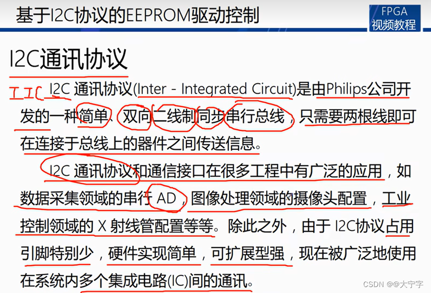
- 1.1 I2C通信协议
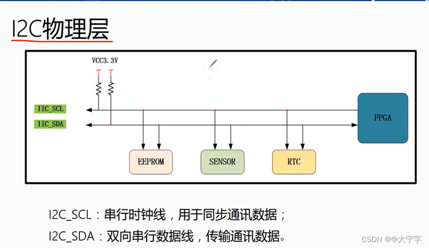
- 1.2 I2C物理层
- 1.3 I2C协议层
- 1.3.1 单字节数据的写入
- 1.3.2 页写数据写入
- 1.3.3 随机读取操作
- 1.3.4 顺序读取操作
- 2. EEPROM
- 2.1 板载 EEPROM 实物图
- 2.2 板载 EEPROM 部分原理图
- 3. 实验目标
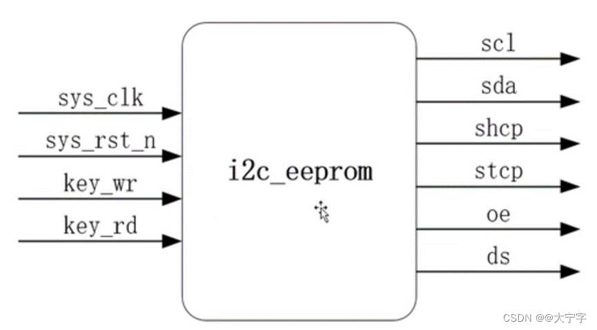
- 4. 模块框图
- 4.1 顶层模块
- 4.2 I2C 驱动模块
- 4.3 数据收发模块
- 5. 波形图
- 5.1 I2C 驱动模块
- 5.2 数据收发模块
- 6. RTL
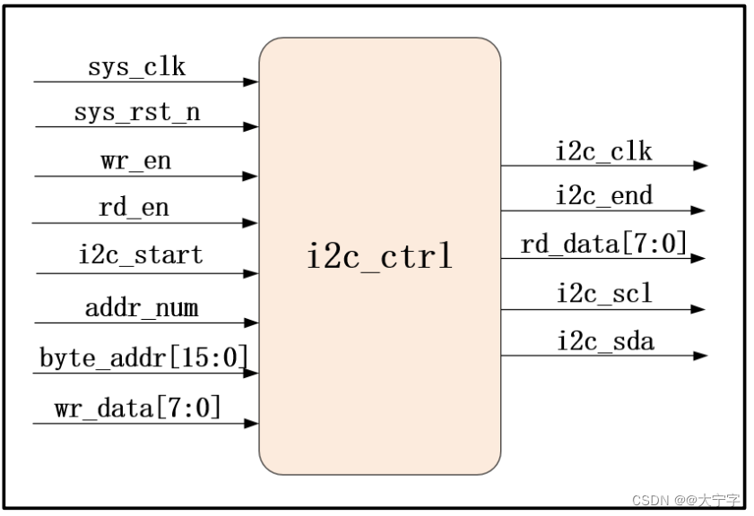
- 6.1 i2c_ctrl
- 6.2 i2c_rw_data
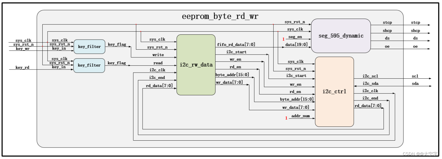
- 6.3 eeprom_byte_rd_wr
- 7. testbench
- 7.1 tb_eeprom_byte_rd_wr
- 7.2 M24LC64
1. I2C协议
1.1 I2C通信协议
1.2 I2C物理层
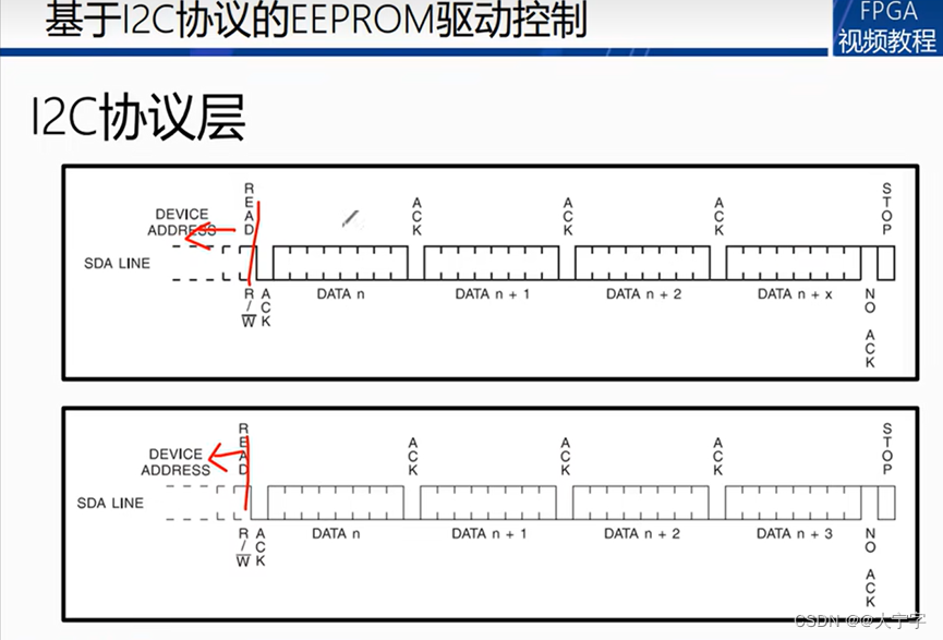
1.3 I2C协议层
1.3.1 单字节数据的写入
单字节地址,2字节地址
1.3.2 页写数据写入
单字节地址,2字节地址
1.3.3 随机读取操作
单字节地址,2字节地址
1.3.4 顺序读取操作
单字节地址,2字节地址
2. EEPROM
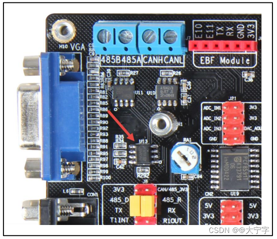
2.1 板载 EEPROM 实物图
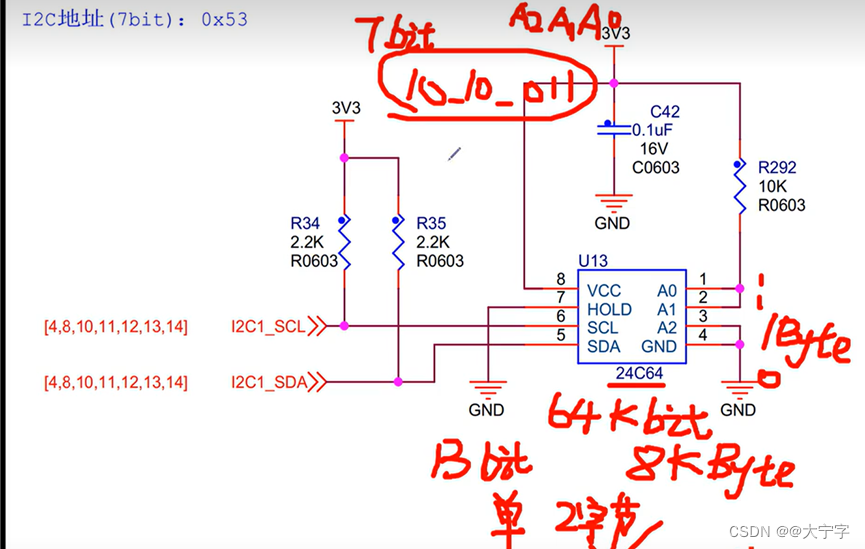
2.2 板载 EEPROM 部分原理图
3. 实验目标
运用所学理论知识设计一个使用 I2C 通讯协议的 EEPROM 读写控制器,使用按键控制数据写入或读出 EEPROM。使用写控制按键向 EEPROM 中写入数据 1-10 共 10 字节数据,使用读控制按键读出之前写入到 EEPROM 的数据,并将读出的数据在数码管上显示出来。
4. 模块框图
4.1 顶层模块
4.2 I2C 驱动模块
4.3 数据收发模块
5. 波形图
5.1 I2C 驱动模块
状态转移图
I2c_scl 250khz 是 i2c_clk的四分频 。串行时钟 scl 的时钟频率为 250KHz,我们要生成的新时钟 i2c_clk 的频率要是 scl 的 4倍,之所以这样是为了后面更好的生成 scl 和 sda,所以 i2c_clk 的时钟频率为 1MHZ。
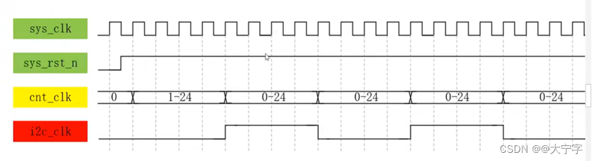
我们使用 50MHz 系统时钟生成了 1MHz 时钟 i2c_clk,但输出至 EEPROM 的串行时钟scl 的时钟频率为 250KHz,我们声明时钟信号计数器 cnt_i2c_clk,作为分频计数器,对时钟 i2c_clk 时钟信号进行计数,初值为 0,计数范围为 0-3,计数时钟为 i2c_clk 时钟,每个时钟周期自加 1,实现时钟 i2c_clk 信号的 4 分频,生成串行时钟 scl。同时计数器cnt_i2c_clk 也可作为生成串行数据 sda 的约束条件,以及状态机跳转条件。
 当Sda_en高电平 sda_out 输出 当 Sda_en 低电平sda_out 低电平 当 sda_en 为高电平 i2c_scl = sda_out 当为低电平时候 i2c_scl = 0
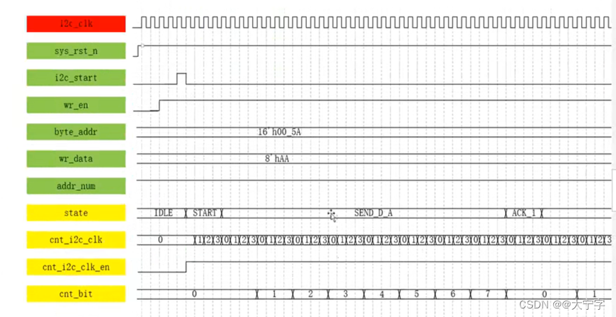
随机读操作整体波形图
5.2 数据收发模块
跨时钟阈的处理,用低频的信号去采集高频的信号,延长有效信号。
三个字节的写入
读操作的波形图
6. RTL
6.1 i2c_ctrl
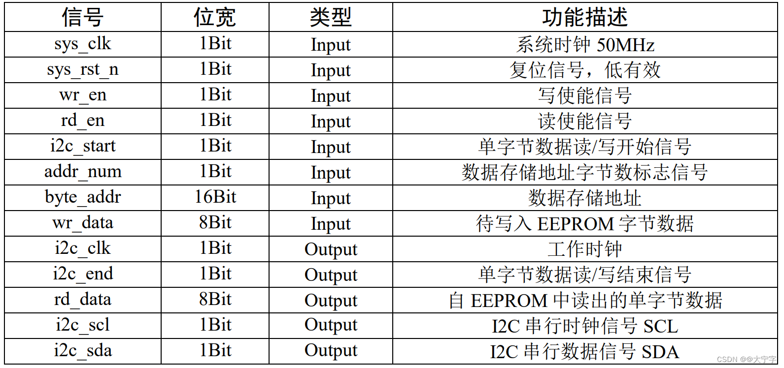
`timescale 1ns/1ns
module i2c_ctrl
#(
parameter DEVICE_ADDR = 7'b1010_000 , //i2c设备地址
parameter SYS_CLK_FREQ = 26'd50_000_000 , //输入系统时钟频率
parameter SCL_FREQ = 18'd250_000 //i2c设备scl时钟频率
)
(
input wire sys_clk , //输入系统时钟,50MHz
input wire sys_rst_n , //输入复位信号,低电平有效
input wire wr_en , //输入写使能信号
input wire rd_en , //输入读使能信号
input wire i2c_start , //输入i2c触发信号
input wire addr_num , //输入i2c字节地址字节数
input wire [15:0] byte_addr , //输入i2c字节地址
input wire [7:0] wr_data , //输入i2c设备数据
output reg i2c_clk , //i2c驱动时钟
output reg i2c_end , //i2c一次读/写操作完成
output reg [7:0] rd_data , //输出i2c设备读取数据
output reg i2c_scl , //输出至i2c设备的串行时钟信号scl
inout wire i2c_sda //输出至i2c设备的串行数据信号sda
);
//************************************************************************//
//******************** Parameter and Internal Signal *********************//
//************************************************************************//
// parameter define
parameter CNT_CLK_MAX = (SYS_CLK_FREQ/SCL_FREQ) >> 2'd3 ; //cnt_clk计数器计数最大值
parameter CNT_START_MAX = 8'd100; //cnt_start计数器计数最大值
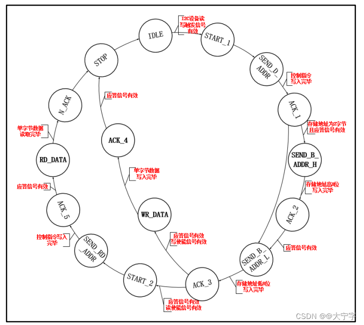
parameter IDLE = 4'd00, //初始状态
START_1 = 4'd01, //开始状态1
SEND_D_ADDR = 4'd02, //设备地址写入状态 + 控制写
ACK_1 = 4'd03, //应答状态1
SEND_B_ADDR_H = 4'd04, //字节地址高八位写入状态
ACK_2 = 4'd05, //应答状态2
SEND_B_ADDR_L = 4'd06, //字节地址低八位写入状态
ACK_3 = 4'd07, //应答状态3
WR_DATA = 4'd08, //写数据状态
ACK_4 = 4'd09, //应答状态4
START_2 = 4'd10, //开始状态2
SEND_RD_ADDR = 4'd11, //设备地址写入状态 + 控制读
ACK_5 = 4'd12, //应答状态5
RD_DATA = 4'd13, //读数据状态
N_ACK = 4'd14, //非应答状态
STOP = 4'd15; //结束状态
// wire define
wire sda_in ; //sda输入数据寄存
wire sda_en ; //sda数据写入使能信号
// reg define
reg [7:0] cnt_clk ; //系统时钟计数器,控制生成clk_i2c时钟信号
reg [3:0] state ; //状态机状态
reg cnt_i2c_clk_en ; //cnt_i2c_clk计数器使能信号
reg [1:0] cnt_i2c_clk ; //clk_i2c时钟计数器,控制生成cnt_bit信号
reg [2:0] cnt_bit ; //sda比特计数器
reg ack ; //应答信号
reg i2c_sda_reg ; //sda数据缓存
reg [7:0] rd_data_reg ; //自i2c设备读出数据
//************************************************************************//
//******************************* Main Code ******************************//
//************************************************************************//
// cnt_clk:系统时钟计数器,控制生成clk_i2c时钟信号
always@(posedge sys_clk or negedge sys_rst_n)
if(sys_rst_n == 1'b0)
cnt_clk <= 8'd0;
else if(cnt_clk == CNT_CLK_MAX - 1'b1)
cnt_clk <= 8'd0;
else
cnt_clk <= cnt_clk + 1'b1;
// i2c_clk:i2c驱动时钟
always@(posedge sys_clk or negedge sys_rst_n)
if(sys_rst_n == 1'b0)
i2c_clk <= 1'b1;
else if(cnt_clk == CNT_CLK_MAX - 1'b1)
i2c_clk <= ~i2c_clk;
// cnt_i2c_clk_en:cnt_i2c_clk计数器使能信号
always@(posedge i2c_clk or negedge sys_rst_n)
if(sys_rst_n == 1'b0)
cnt_i2c_clk_en <= 1'b0;
else if((state == STOP) && (cnt_bit == 3'd3) &&(cnt_i2c_clk == 3))
cnt_i2c_clk_en <= 1'b0;
else if(i2c_start == 1'b1)
cnt_i2c_clk_en <= 1'b1;
// cnt_i2c_clk:i2c_clk时钟计数器,控制生成cnt_bit信号
always@(posedge i2c_clk or negedge sys_rst_n)
if(sys_rst_n == 1'b0)
cnt_i2c_clk <= 2'd0;
else if(cnt_i2c_clk_en == 1'b1)
cnt_i2c_clk <= cnt_i2c_clk + 1'b1;
// cnt_bit:sda比特计数器
always@(posedge i2c_clk or negedge sys_rst_n)
if(sys_rst_n == 1'b0)
cnt_bit <= 3'd0;
else if((state == IDLE) || (state == START_1) || (state == START_2)
|| (state == ACK_1) || (state == ACK_2) || (state == ACK_3)
|| (state == ACK_4) || (state == ACK_5) || (state == N_ACK))
cnt_bit <= 3'd0;
else if((cnt_bit == 3'd7) && (cnt_i2c_clk == 2'd3))
cnt_bit <= 3'd0;
else if((cnt_i2c_clk == 2'd3) && (state != IDLE))
cnt_bit <= cnt_bit + 1'b1;
// state:状态机状态跳转
always@(posedge i2c_clk or negedge sys_rst_n)
if(sys_rst_n == 1'b0)
state <= IDLE;
else case(state)
IDLE:
if(i2c_start == 1'b1)
state <= START_1;
else
state <= state;
START_1:
if(cnt_i2c_clk == 3)
state <= SEND_D_ADDR;
else
state <= state;
SEND_D_ADDR:
if((cnt_bit == 3'd7) &&(cnt_i2c_clk == 3))
state <= ACK_1;
else
state <= state;
ACK_1:
if((cnt_i2c_clk == 3) && (ack == 1'b0))
begin
if(addr_num == 1'b1)
state <= SEND_B_ADDR_H;
else
state <= SEND_B_ADDR_L;
end
else
state <= state;
SEND_B_ADDR_H:
if((cnt_bit == 3'd7) &&(cnt_i2c_clk == 3))
state <= ACK_2;
else
state <= state;
ACK_2:
if((cnt_i2c_clk == 3) && (ack == 1'b0))
state <= SEND_B_ADDR_L;
else
state <= state;
SEND_B_ADDR_L:
if((cnt_bit == 3'd7) && (cnt_i2c_clk == 3))
state <= ACK_3;
else
state <= state;
ACK_3:
if((cnt_i2c_clk == 3) && (ack == 1'b0))
begin
if(wr_en == 1'b1)
state <= WR_DATA;
else if(rd_en == 1'b1)
state <= START_2;
else
state <= state;
end
else
state <= state;
WR_DATA:
if((cnt_bit == 3'd7) &&(cnt_i2c_clk == 3))
state <= ACK_4;
else
state <= state;
ACK_4:
if((cnt_i2c_clk == 3) && (ack == 1'b0))
state <= STOP;
else
state <= state;
START_2:
if(cnt_i2c_clk == 3)
state <= SEND_RD_ADDR;
else
state <= state;
SEND_RD_ADDR:
if((cnt_bit == 3'd7) &&(cnt_i2c_clk == 3))
state <= ACK_5;
else
state <= state;
ACK_5:
if((cnt_i2c_clk == 3) && (ack == 1'b0))
state <= RD_DATA;
else
state <= state;
RD_DATA:
if((cnt_bit == 3'd7) &&(cnt_i2c_clk == 3))
state <= N_ACK;
else
state <= state;
N_ACK:
if(cnt_i2c_clk == 3)
state <= STOP;
else
state <= state;
STOP:
if((cnt_bit == 3'd3) &&(cnt_i2c_clk == 3))
state <= IDLE;
else
state <= state;
default: state <= IDLE;
endcase
// ack:应答信号
always@(*)
case (state)
IDLE,START_1,SEND_D_ADDR,SEND_B_ADDR_H,SEND_B_ADDR_L,
WR_DATA,START_2,SEND_RD_ADDR,RD_DATA,N_ACK:
ack <= 1'b1;
ACK_1,ACK_2,ACK_3,ACK_4,ACK_5:
if(cnt_i2c_clk == 2'd0)
ack <= sda_in;
else
ack <= ack;
default: ack <= 1'b1;
endcase
// i2c_scl:输出至i2c设备的串行时钟信号scl
always@(*)
case (state)
IDLE:
i2c_scl <= 1'b1;
START_1:
if(cnt_i2c_clk == 2'd3)
i2c_scl <= 1'b0;
else
i2c_scl <= 1'b1;
SEND_D_ADDR,ACK_1,SEND_B_ADDR_H,ACK_2,SEND_B_ADDR_L,
ACK_3,WR_DATA,ACK_4,START_2,SEND_RD_ADDR,ACK_5,RD_DATA,N_ACK:
if((cnt_i2c_clk == 2'd1) || (cnt_i2c_clk == 2'd2))
i2c_scl <= 1'b1;
else
i2c_scl <= 1'b0;
STOP:
if((cnt_bit == 3'd0) &&(cnt_i2c_clk == 2'd0))
i2c_scl <= 1'b0;
else
i2c_scl <= 1'b1;
default: i2c_scl <= 1'b1;
endcase
// i2c_sda_reg:sda数据缓存
always@(*)
case (state)
IDLE:
begin
i2c_sda_reg <= 1'b1;
rd_data_reg <= 8'd0;
end
START_1:
if(cnt_i2c_clk <= 2'd0)
i2c_sda_reg <= 1'b1;
else
i2c_sda_reg <= 1'b0;
SEND_D_ADDR:
if(cnt_bit <= 3'd6)
i2c_sda_reg <= DEVICE_ADDR[6 - cnt_bit];
else
i2c_sda_reg <= 1'b0;
ACK_1:
i2c_sda_reg <= 1'b1;
SEND_B_ADDR_H:
i2c_sda_reg <= byte_addr[15 - cnt_bit];
ACK_2:
i2c_sda_reg <= 1'b1;
SEND_B_ADDR_L:
i2c_sda_reg <= byte_addr[7 - cnt_bit];
ACK_3:
i2c_sda_reg <= 1'b1;
WR_DATA:
i2c_sda_reg <= wr_data[7 - cnt_bit];
ACK_4:
i2c_sda_reg <= 1'b1;
START_2:
if(cnt_i2c_clk <= 2'd1)
i2c_sda_reg <= 1'b1;
else
i2c_sda_reg <= 1'b0;
SEND_RD_ADDR:
if(cnt_bit <= 3'd6)
i2c_sda_reg <= DEVICE_ADDR[6 - cnt_bit];
else
i2c_sda_reg <= 1'b1;
ACK_5:
i2c_sda_reg <= 1'b1;
RD_DATA:
if(cnt_i2c_clk == 2'd2)
rd_data_reg[7 - cnt_bit] <= sda_in;
else
rd_data_reg <= rd_data_reg;
N_ACK:
i2c_sda_reg <= 1'b1;
STOP:
if((cnt_bit == 3'd0) && (cnt_i2c_clk < 2'd3))
i2c_sda_reg <= 1'b0;
else
i2c_sda_reg <= 1'b1;
default:
begin
i2c_sda_reg <= 1'b1;
rd_data_reg <= rd_data_reg;
end
endcase
// rd_data:自i2c设备读出数据
always@(posedge i2c_clk or negedge sys_rst_n)
if(sys_rst_n == 1'b0)
rd_data <= 8'd0;
else if((state == RD_DATA) && (cnt_bit == 3'd7) && (cnt_i2c_clk == 2'd3))
rd_data <= rd_data_reg;
// i2c_end:一次读/写结束信号
always@(posedge i2c_clk or negedge sys_rst_n)
if(sys_rst_n == 1'b0)
i2c_end <= 1'b0;
else if((state == STOP) && (cnt_bit == 3'd3) &&(cnt_i2c_clk == 3))
i2c_end <= 1'b1;
else
i2c_end <= 1'b0;
// sda_in:sda输入数据寄存
assign sda_in = i2c_sda;
// sda_en:sda数据写入使能信号
assign sda_en = ((state == RD_DATA) || (state == ACK_1) || (state == ACK_2)
|| (state == ACK_3) || (state == ACK_4) || (state == ACK_5))
? 1'b0 : 1'b1;
// i2c_sda:输出至i2c设备的串行数据信号sda
assign i2c_sda = (sda_en == 1'b1) ? i2c_sda_reg : 1'bz;
endmodule
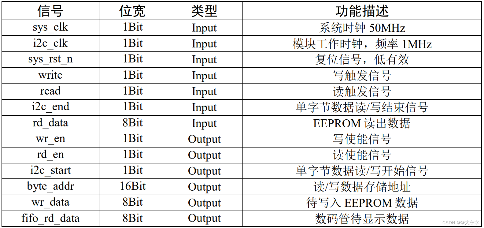
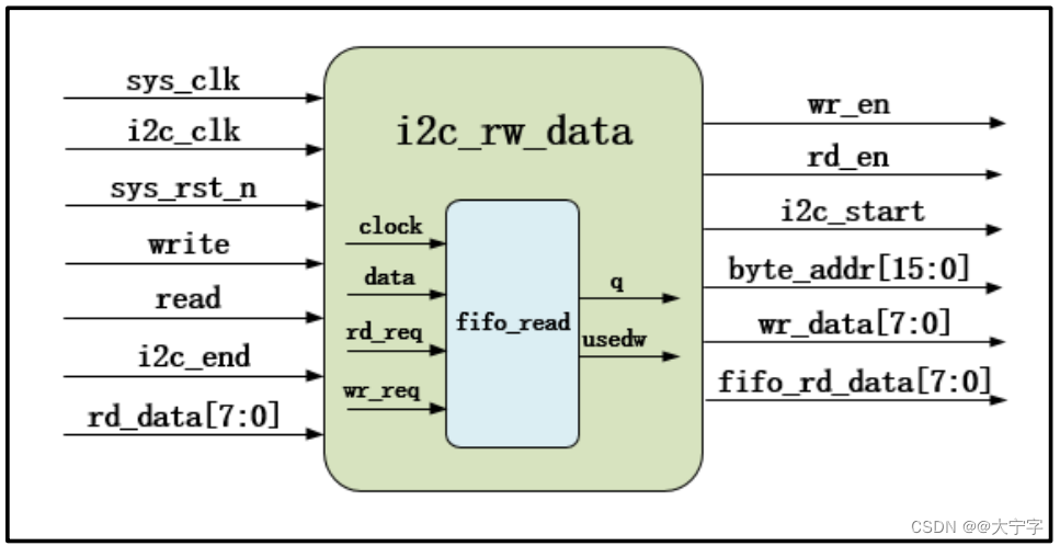
6.2 i2c_rw_data
`timescale  1ns/1ns


module  i2c_rw_data
(
    input   wire            sys_clk     ,   //输入系统时钟,频率50MHz
    input   wire            i2c_clk     ,   //输入i2c驱动时钟,频率1MHz
    input   wire            sys_rst_n   ,   //输入复位信号,低有效
    input   wire            write       ,   //输入写触发信号
    input   wire            read        ,   //输入读触发信号
    input   wire            i2c_end     ,   //一次i2c读/写结束信号
    input   wire    [7:0]   rd_data     ,   //输入自i2c设备读出的数据

    output  reg             wr_en       ,   //输出写使能信号
    output  reg             rd_en       ,   //输出读使能信号
    output  reg             i2c_start   ,   //输出i2c读/写触发信号
    output  reg     [15:0]  byte_addr   ,   //输出i2c设备读/写地址
    output  reg     [7:0]   wr_data     ,   //输出写入i2c设备的数据
    output  wire    [7:0]   fifo_rd_data    //输出自fifo中读出的数据
);

//********************************************************************//
//****************** Parameter and Internal Signal *******************//
//********************************************************************//
// parameter  define
parameter   DATA_NUM        =   8'd10       ,   //读/写操作读出或写入的数据个数
            CNT_START_MAX   =   16'd4000    ,   //cnt_start计数器计数最大值
            CNT_WR_RD_MAX   =   8'd200      ,   //cnt_wr/cnt_rd计数器计数最大值
            CNT_WAIT_MAX    =   28'd500_000 ;   //cnt_wait计数器计数最大值
// wire  define
wire    [7:0]   data_num    ;   //fifo中数据个数

// reg   define
reg     [7:0]   cnt_wr          ;   //写触发有效信号保持时间计数器
reg             write_valid     ;   //写触发有效信号
reg     [7:0]   cnt_rd          ;   //读触发有效信号保持时间计数器
reg             read_valid      ;   //读触发有效信号
reg     [15:0]  cnt_start       ;   //单字节数据读/写时间间隔计数
reg     [7:0]   wr_i2c_data_num ;   //写入i2c设备的数据个数
reg     [7:0]   rd_i2c_data_num ;   //读出i2c设备的数据个数
reg             fifo_rd_valid   ;   //fifo读有效信号
reg     [27:0]  cnt_wait        ;   //fifo读使能信号间时间间隔计数
reg             fifo_rd_en      ;   //fifo读使能信号
reg     [7:0]   rd_data_num     ;   //读出fifo数据个数

//********************************************************************//
//***************************** Main Code ****************************//
//********************************************************************//
//cnt_wr:写触发有效信号保持时间计数器,计数写触发有效信号保持时钟周期数
always@(posedge sys_clk or negedge sys_rst_n)
    if(sys_rst_n == 1'b0)
        cnt_wr    <=  8'd0;
    else    if(write_valid == 1'b0)
        cnt_wr    <=  8'd0;
    else    if(write_valid == 1'b1)
        cnt_wr    <=  cnt_wr + 1'b1;

//write_valid:写触发有效信号
//由于写触发信号保持时间为一个系统时钟周期(20ns),
//不能被i2c驱动时钟i2c_scl正确采集,延长写触发信号生成写触发有效信号
always@(posedge sys_clk or negedge sys_rst_n)
    if(sys_rst_n == 1'b0)
        write_valid    <=  1'b0;
    else    if(cnt_wr == (CNT_WR_RD_MAX - 1'b1))
        write_valid    <=  1'b0;
    else    if(write == 1'b1)
        write_valid    <=  1'b1;

//cnt_rd:读触发有效信号保持时间计数器,计数读触发有效信号保持时钟周期数
always@(posedge sys_clk or negedge sys_rst_n)
    if(sys_rst_n == 1'b0)
        cnt_rd    <=  8'd0;
    else    if(read_valid == 1'b0)
        cnt_rd    <=  8'd0;
    else    if(read_valid == 1'b1)
        cnt_rd    <=  cnt_rd + 1'b1;

//read_valid:读触发有效信号
//由于读触发信号保持时间为一个系统时钟周期(20ns),
//不能被i2c驱动时钟i2c_scl正确采集,延长读触发信号生成读触发有效信号
always@(posedge sys_clk or negedge sys_rst_n)
    if(sys_rst_n == 1'b0)
        read_valid    <=  1'b0;
    else    if(cnt_rd == (CNT_WR_RD_MAX - 1'b1))
        read_valid    <=  1'b0;
    else    if(read == 1'b1)
        read_valid    <=  1'b1;

//cnt_start:单字节数据读/写操作时间间隔计数
always@(posedge i2c_clk or negedge sys_rst_n)
    if(sys_rst_n == 1'b0)
        cnt_start   <=  16'd0;
    else    if((wr_en == 1'b0) && (rd_en == 1'b0))
        cnt_start   <=  16'd0;
    else    if(cnt_start == (CNT_START_MAX - 1'b1))
        cnt_start   <=  16'd0;
    else    if((wr_en == 1'b1) || (rd_en == 1'b1))
        cnt_start   <=  cnt_start + 1'b1;

//i2c_start:i2c读/写触发信号
always@(posedge i2c_clk or negedge sys_rst_n)
    if(sys_rst_n == 1'b0)
        i2c_start   <=  1'b0;
    else    if((cnt_start == (CNT_START_MAX - 1'b1)))
        i2c_start   <=  1'b1;
    else
        i2c_start   <=  1'b0;

//wr_en:输出写使能信号
always@(posedge i2c_clk or negedge sys_rst_n)
    if(sys_rst_n == 1'b0)
        wr_en   <=  1'b0;
    else    if((wr_i2c_data_num == DATA_NUM - 1)
                && (i2c_end == 1'b1) && (wr_en == 1'b1))
        wr_en   <=  1'b0;
    else    if(write_valid == 1'b1)
        wr_en   <=  1'b1;

//wr_i2c_data_num:写入i2c设备的数据个数
always@(posedge i2c_clk or negedge sys_rst_n)
    if(sys_rst_n == 1'b0)
        wr_i2c_data_num <=  8'd0;
    else    if(wr_en == 1'b0)
        wr_i2c_data_num <=  8'd0;
    else    if((wr_en == 1'b1) && (i2c_end == 1'b1))
        wr_i2c_data_num <=  wr_i2c_data_num + 1'b1;

//rd_en:输出读使能信号
always@(posedge i2c_clk or negedge sys_rst_n)
    if(sys_rst_n == 1'b0)
        rd_en   <=  1'b0;
    else    if((rd_i2c_data_num == DATA_NUM - 1)
                && (i2c_end == 1'b1) && (rd_en == 1'b1))
        rd_en   <=  1'b0;
    else    if(read_valid == 1'b1)
        rd_en   <=  1'b1;

//rd_i2c_data_num:写入i2c设备的数据个数
always@(posedge i2c_clk or negedge sys_rst_n)
    if(sys_rst_n == 1'b0)
        rd_i2c_data_num <=  8'd0;
    else    if(rd_en == 1'b0)
        rd_i2c_data_num <=  8'd0;
    else    if((rd_en == 1'b1) && (i2c_end == 1'b1))
        rd_i2c_data_num <=  rd_i2c_data_num + 1'b1;

//byte_addr:输出读/写地址
always@(posedge i2c_clk or negedge sys_rst_n)
    if(sys_rst_n == 1'b0)
        byte_addr   <=  16'h00_5A;
    else    if((wr_en == 1'b0) && (rd_en == 1'b0))
        byte_addr   <=  16'h00_5A;
    else    if(((wr_en == 1'b1) || (rd_en == 1'b1)) && (i2c_end == 1'b1))
        byte_addr   <=  byte_addr + 1'b1;

//wr_data:输出待写入i2c设备数据
always@(posedge i2c_clk or negedge sys_rst_n)
    if(sys_rst_n == 1'b0)
        wr_data <=  8'h01;
    else    if(wr_en == 1'b0)
        wr_data <=  8'h01;
    else    if((wr_en == 1'b1) && (i2c_end == 1'b1))
        wr_data <=  wr_data + 1'b1;

//fifo_rd_valid:fifo读有效信号
always@(posedge i2c_clk or negedge sys_rst_n)
    if(sys_rst_n == 1'b0)
        fifo_rd_valid  <=  1'b0;
    else    if((rd_data_num == DATA_NUM)
                && (cnt_wait == (CNT_WAIT_MAX - 1'b1)))
        fifo_rd_valid  <=  1'b0;
    else    if(data_num == DATA_NUM)
        fifo_rd_valid  <=  1'b1;

//cnt_wait:fifo读使能信号间时间间隔计数,计数两fifo读使能间的时间间隔
always@(posedge i2c_clk or negedge sys_rst_n)
    if(sys_rst_n == 1'b0)
        cnt_wait    <=  28'd0;
    else    if(fifo_rd_valid == 1'b0)
        cnt_wait    <=  28'd0;
    else    if(cnt_wait == (CNT_WAIT_MAX - 1'b1))
        cnt_wait    <=  28'd0;
    else    if(fifo_rd_valid == 1'b1)
        cnt_wait    <=  cnt_wait + 1'b1;

//fifo_rd_en:fifo读使能信号
always@(posedge i2c_clk or negedge sys_rst_n)
    if(sys_rst_n == 1'b0)
        fifo_rd_en <=  1'b0;
    else    if((cnt_wait == (CNT_WAIT_MAX - 1'b1))
                && (rd_data_num < DATA_NUM))
        fifo_rd_en <=  1'b1;
    else
        fifo_rd_en <=  1'b0;

//rd_data_num:自fifo中读出数据个数计数
always@(posedge i2c_clk or negedge sys_rst_n)
    if(sys_rst_n == 1'b0)
        rd_data_num <=  8'd0;
    else    if(fifo_rd_valid == 1'b0)
        rd_data_num <=  8'd0;
    else    if(fifo_rd_en == 1'b1)
        rd_data_num <=  rd_data_num + 1'b1;

//****************************************************************//
//************************* Instantiation ************************//
//****************************************************************//
//------------- fifo_read_inst -------------
fifo_data   fifo_read_inst
(
    .clock  (i2c_clk            ),  //输入时钟信号,频率1MHz,1bit
    .data   (rd_data            ),  //输入写入数据,1bit
    .rdreq  (fifo_rd_en         ),  //输入数据读请求,1bit
    .wrreq  (i2c_end && rd_en   ),  //输入数据写请求,1bit

    .q      (fifo_rd_data       ),  //输出读出数据,1bit
    .usedw  (data_num           )   //输出fifo内数据个数,1bit
);

endmodule
6.3 eeprom_byte_rd_wr
`timescale  1ns/1ns


module  eeprom_byte_rd_wr
(
    input   wire            sys_clk     ,   //输入工作时钟,频率50MHz
    input   wire            sys_rst_n   ,   //输入复位信号,低电平有效
    input   wire            key_wr      ,   //按键写
    input   wire            key_rd      ,   //按键读

    inout   wire            sda         ,   //串行数据
    output  wire            scl         ,   //串行时钟
    output  wire            stcp        ,   //输出数据存储器时钟
    output  wire            shcp        ,   //移位寄存器的时钟输入
    output  wire            ds          ,   //串行数据输入
    output  wire            oe              //使能信号
);

//********************************************************************//
//****************** Parameter and Internal Signal *******************//
//********************************************************************//
//wire  define
wire            read        ;   //读数据
wire            write       ;   //写数据
wire    [7:0]   po_data     ;   //fifo输出数据
wire    [7:0]   rd_data     ;   //eeprom读出数据
wire            wr_en       ;
wire            rd_en       ;
wire            i2c_end     ;
wire            i2c_start   ;
wire    [7:0]   wr_data     ;
wire    [15:0]  byte_addr   ;
wire            i2c_clk     ;

//********************************************************************//
//*************************** Instantiation **************************//
//********************************************************************//
//------------- key_wr_inst -------------
key_filter  key_wr_inst
(
    .sys_clk    (sys_clk    ),  //系统时钟50Mhz
    .sys_rst_n  (sys_rst_n  ),  //全局复位
    .key_in     (key_wr     ),  //按键输入信号

    .key_flag   (write      )   //key_flag为1时表示按键有效,0表示按键无效
);

//------------- key_rd_inst -------------
key_filter  key_rd_inst
(
    .sys_clk    (sys_clk    ),  //系统时钟50Mhz
    .sys_rst_n  (sys_rst_n  ),  //全局复位
    .key_in     (key_rd     ),  //按键输入信号

    .key_flag   (read       )   //key_flag为1时表示按键有效,0表示按键无效
);

//------------- i2c_rw_data_inst -------------
i2c_rw_data i2c_rw_data_inst
(
    .sys_clk     (sys_clk   ),  //输入系统时钟,频率50MHz
    .i2c_clk     (i2c_clk   ),  //输入i2c驱动时钟,频率1MHz
    .sys_rst_n   (sys_rst_n ),  //输入复位信号,低有效
    .write       (write     ),  //输入写触发信号
    .read        (read      ),  //输入读触发信号
    .i2c_end     (i2c_end   ),  //一次i2c读/写结束信号
    .rd_data     (rd_data   ),  //输入自i2c设备读出的数据

    .wr_en       (wr_en     ),  //输出写使能信号
    .rd_en       (rd_en     ),  //输出读使能信号
    .i2c_start   (i2c_start ),  //输出i2c读/写触发信号
    .byte_addr   (byte_addr ),  //输出i2c设备读/写地址
    .wr_data     (wr_data   ),  //输出写入i2c设备的数据
    .fifo_rd_data(po_data   )   //输出自fifo中读出的数据

);

//------------- i2c_ctrl_inst -------------
i2c_ctrl
#(
    .DEVICE_ADDR    (7'b1010_011     ), //i2c设备器件地址
    .SYS_CLK_FREQ   (26'd50_000_000  ), //i2c_ctrl模块系统时钟频率
    .SCL_FREQ       (18'd250_000     )  //i2c的SCL时钟频率
)
i2c_ctrl_inst
(
    .sys_clk     (sys_clk   ),   //输入系统时钟,50MHz
    .sys_rst_n   (sys_rst_n ),   //输入复位信号,低电平有效
    .wr_en       (wr_en     ),   //输入写使能信号
    .rd_en       (rd_en     ),   //输入读使能信号
    .i2c_start   (i2c_start ),   //输入i2c触发信号
    .addr_num    (1'b1      ),   //输入i2c字节地址字节数
    .byte_addr   (byte_addr ),   //输入i2c字节地址
    .wr_data     (wr_data   ),   //输入i2c设备数据

    .rd_data     (rd_data   ),   //输出i2c设备读取数据
    .i2c_end     (i2c_end   ),   //i2c一次读/写操作完成
    .i2c_clk     (i2c_clk   ),   //i2c驱动时钟
    .i2c_scl     (scl       ),   //输出至i2c设备的串行时钟信号scl
    .i2c_sda     (sda       )    //输出至i2c设备的串行数据信号sda
);

//------------- seg7_dynamic_inst -------------
seg_595_dynamic seg_595_dynamic_inst
(
    .sys_clk     (sys_clk   ), //系统时钟,频率50MHz
    .sys_rst_n   (sys_rst_n ), //复位信号,低有效
    .data        (po_data   ), //数码管要显示的值
    .point       (          ), //小数点显示,高电平有效
    .seg_en      (1'b1      ), //数码管使能信号,高电平有效
    .sign        (          ), //符号位,高电平显示负号

    .stcp        (stcp      ), //数据存储器时钟
    .shcp        (shcp      ), //移位寄存器时钟
    .ds          (ds        ), //串行数据输入
    .oe          (oe        )  //使能信号
);

endmodule
7. testbench
7.1 tb_eeprom_byte_rd_wr
`timescale  1ns/1ns


module  tb_eeprom_byte_rd_wr();
//wire define
wire            scl ;
wire            sda ;
wire            stcp;
wire            shcp;
wire            ds  ;
wire            oe  ;

//reg define
reg           clk   ;
reg           rst_n ;
reg           key_wr;
reg           key_rd;

//时钟、复位信号
initial
  begin
    clk     =   1'b1  ;
    rst_n   <=  1'b0  ;
    key_wr  <=  1'b1  ;
    key_rd  <=  1'b1  ;
    #200
    rst_n   <=  1'b1  ;
    #1000
    key_wr  <=  1'b0  ;
    key_rd  <=  1'b1  ;
    #400
    key_wr  <=  1'b1  ;
    key_rd  <=  1'b1  ;
    #20000000
    key_wr  <=  1'b1  ;
    key_rd  <=  1'b0  ;
    #400
    key_wr  <=  1'b1  ;
    key_rd  <=  1'b1  ;
    #40000000
    $stop;
  end

always  #10 clk = ~clk;

defparam eeprom_byte_rd_wr_inst.key_wr_inst.CNT_MAX = 5;
defparam eeprom_byte_rd_wr_inst.key_rd_inst.CNT_MAX = 5;
defparam eeprom_byte_rd_wr_inst.i2c_rw_data_inst.CNT_WAIT_MAX = 1000;

//-------------eeprom_byte_rd_wr_inst-------------
eeprom_byte_rd_wr   eeprom_byte_rd_wr_inst
(
    .sys_clk        (clk    ),    //输入工作时钟,频率50MHz
    .sys_rst_n      (rst_n  ),    //输入复位信号,低电平有效
    .key_wr         (key_wr ),    //按键写
    .key_rd         (key_rd ),    //按键读

    .sda            (sda    ),    //串行数据
    .scl            (scl    ),    //串行时钟
    .stcp           (stcp   ),   //输出数据存储寄时钟
    .shcp           (shcp   ),   //移位寄存器的时钟输入
    .ds             (ds     ),   //串行数据输入
    .oe             (oe     )

);

//-------------eeprom_inst-------------
M24LC64  M24lc64_inst
(
    .A0     (1'b0       ),  //器件地址
    .A1     (1'b0       ),  //器件地址
    .A2     (1'b0       ),  //器件地址
    .WP     (1'b0       ),  //写保护信号,高电平有效
    .RESET  (~rst_n     ),  //复位信号,高电平有效

    .SDA    (sda        ),  //串行数据
    .SCL    (scl        )   //串行时钟
);

endmodule
7.2 M24LC64
// *******************************************************************************************************
// ** **
// ** 24LC64.v - Microchip 24LC64 64K-BIT I2C SERIAL EEPROM (VCC = +2.5V TO +5.5V) **
// ** **
// *******************************************************************************************************
// ** **
// ** This information is distributed under license from Young Engineering. **
// ** COPYRIGHT (c) 2009 YOUNG ENGINEERING **
// ** ALL RIGHTS RESERVED **
// ** **
// ** **
// ** Young Engineering provides design expertise for the digital world **
// ** Started in 1990, Young Engineering offers products and services for your electronic design **
// ** project. We have the expertise in PCB, FPGA, ASIC, firmware, and software design. **
// ** From concept to prototype to production, we can help you. **
// ** **
// ** http://www.young-engineering.com/ **
// ** **
// *******************************************************************************************************
// ** This information is provided to you for your convenience and use with Microchip products only. **
// ** Microchip disclaims all liability arising from this information and its use. **
// ** **
// ** THIS INFORMATION IS PROVIDED "AS IS." MICROCHIP MAKES NO REPRESENTATION OR WARRANTIES OF **
// ** ANY KIND WHETHER EXPRESS OR IMPLIED, WRITTEN OR ORAL, STATUTORY OR OTHERWISE, RELATED TO **
// ** THE INFORMATION PROVIDED TO YOU, INCLUDING BUT NOT LIMITED TO ITS CONDITION, QUALITY, **
// ** PERFORMANCE, MERCHANTABILITY, NON-INFRINGEMENT, OR FITNESS FOR PURPOSE. **
// ** MICROCHIP IS NOT LIABLE, UNDER ANY CIRCUMSTANCES, FOR SPECIAL, INCIDENTAL OR CONSEQUENTIAL **
// ** DAMAGES, FOR ANY REASON WHATSOEVER. **
// ** **
// ** It is your responsibility to ensure that your application meets with your specifications. **
// ** **
// *******************************************************************************************************
// ** Revision : 1.4 **
// ** Modified Date : 02/04/2009 **
// ** Revision History: **
// ** **
// ** 10/01/2003: Initial design **
// ** 07/19/2004: Fixed the timing checks and the open-drain modeling for SDA. **
// ** 01/06/2006: Changed the legal information in the header **
// ** 12/04/2006: Corrected timing checks to reference proper clock edges **
// ** Added timing check for Tbuf (bus free time) **
// ** Reduced memory blocks to single, monolithic array **
// ** 02/04/2009: Added timing checks for tSU_WP and tHD_WP **
// ** **
// *******************************************************************************************************
// ** TABLE OF CONTENTS **
// *******************************************************************************************************
// **---------------------------------------------------------------------------------------------------**
// ** DECLARATIONS **
// **---------------------------------------------------------------------------------------------------**
// **---------------------------------------------------------------------------------------------------**
// ** INITIALIZATION **
// **---------------------------------------------------------------------------------------------------**
// **---------------------------------------------------------------------------------------------------**
// ** CORE LOGIC **
// **---------------------------------------------------------------------------------------------------**
// ** 1.01: START Bit Detection **
// ** 1.02: STOP Bit Detection **
// ** 1.03: Input Shift Register **
// ** 1.04: Input Bit Counter **
// ** 1.05: Control Byte Register **
// ** 1.06: Byte Address Register **
// ** 1.07: Write Data Buffer **
// ** 1.08: Acknowledge Generator **
// ** 1.09: Acknowledge Detect **
// ** 1.10: Write Cycle Timer **
// ** 1.11: Write Cycle Processor **
// ** 1.12: Read Data Multiplexor **
// ** 1.13: Read Data Processor **
// ** 1.14: SDA Data I/O Buffer **
// ** **
// **---------------------------------------------------------------------------------------------------**
// ** DEBUG LOGIC **
// **---------------------------------------------------------------------------------------------------**
// ** 2.01: Memory Data Bytes **
// ** 2.02: Write Data Buffer **
// ** **
// **---------------------------------------------------------------------------------------------------**
// ** TIMING CHECKS **
// **---------------------------------------------------------------------------------------------------**
// ** **
// *******************************************************************************************************
`timescale 1ns/10ps
module M24LC64 (A0, A1, A2, WP, SDA, SCL, RESET);
input A0; // chip select bit
input A1; // chip select bit
input A2; // chip select bit
input WP; // write protect pin
inout SDA; // serial data I/O
input SCL; // serial data clock
input RESET; // system reset
// *******************************************************************************************************
// ** DECLARATIONS **
// *******************************************************************************************************
reg SDA_DO; // serial data - output
reg SDA_OE; // serial data - output enable
wire SDA_DriveEnable; // serial data output enable
reg SDA_DriveEnableDlyd; // serial data output enable - delayed
wire [02:00] ChipAddress; // hardwired chip address
reg [03:00] BitCounter; // serial bit counter
reg START_Rcvd; // START bit received flag
reg STOP_Rcvd; // STOP bit received flag
reg CTRL_Rcvd; // control byte received flag
reg ADHI_Rcvd; // byte address hi received flag
reg ADLO_Rcvd; // byte address lo received flag
reg MACK_Rcvd; // master acknowledge received flag
reg WrCycle; // memory write cycle
reg RdCycle; // memory read cycle
reg [07:00] ShiftRegister; // input data shift register
reg [07:00] ControlByte; // control byte register
wire RdWrBit; // read/write control bit
reg [12:00] StartAddress; // memory access starting address
reg [04:00] PageAddress; // memory page address
reg [07:00] WrDataByte [0:31]; // memory write data buffer
wire [07:00] RdDataByte; // memory read data
reg [15:00] WrCounter; // write buffer counter
reg [04:00] WrPointer; // write buffer pointer
reg [12:00] RdPointer; // read address pointer
reg WriteActive; // memory write cycle active
reg [07:00] MemoryBlock [0:8191]; // EEPROM data memory array
integer LoopIndex; // iterative loop index
integer tAA; // timing parameter
integer tWC; // timing parameter
// *******************************************************************************************************
// ** INITIALIZATION **
// *******************************************************************************************************
//----------------------------
//------写数据间隔改动----------
initial tAA = 900; // SCL to SDA output delay
initial tWC = 500; // memory write cycle time
// initial tAA = 900; // SCL to SDA output delay
// initial tWC = 5000000; // memory write cycle time
initial begin
SDA_DO = 0;
SDA_OE = 0;
end
initial begin
START_Rcvd = 0;
STOP_Rcvd = 0;
CTRL_Rcvd = 0;
ADHI_Rcvd = 0;
ADLO_Rcvd = 0;
MACK_Rcvd = 0;
end
initial begin
BitCounter = 0;
ControlByte = 0;
end
initial begin
WrCycle = 0;
RdCycle = 0;
WriteActive = 0;
end
assign ChipAddress = {A2,A1,A0};
// *******************************************************************************************************
// ** CORE LOGIC **
// *******************************************************************************************************
// -------------------------------------------------------------------------------------------------------
// 1.01: START Bit Detection
// -------------------------------------------------------------------------------------------------------
always @(negedge SDA) begin
if (SCL == 1) begin
START_Rcvd <= 1;
STOP_Rcvd <= 0;
CTRL_Rcvd <= 0;
ADHI_Rcvd <= 0;
ADLO_Rcvd <= 0;
MACK_Rcvd <= 0;
WrCycle <= #1 0;
RdCycle <= #1 0;
BitCounter <= 0;
end
end
// -------------------------------------------------------------------------------------------------------
// 1.02: STOP Bit Detection
// -------------------------------------------------------------------------------------------------------
always @(posedge SDA) begin
if (SCL == 1) begin
START_Rcvd <= 0;
STOP_Rcvd <= 1;
CTRL_Rcvd <= 0;
ADHI_Rcvd <= 0;
ADLO_Rcvd <= 0;
MACK_Rcvd <= 0;
WrCycle <= #1 0;
RdCycle <= #1 0;
BitCounter <= 10;
end
end
// -------------------------------------------------------------------------------------------------------
// 1.03: Input Shift Register
// -------------------------------------------------------------------------------------------------------
always @(posedge SCL) begin
ShiftRegister[00] <= SDA;
ShiftRegister[01] <= ShiftRegister[00];
ShiftRegister[02] <= ShiftRegister[01];
ShiftRegister[03] <= ShiftRegister[02];
ShiftRegister[04] <= ShiftRegister[03];
ShiftRegister[05] <= ShiftRegister[04];
ShiftRegister[06] <= ShiftRegister[05];
ShiftRegister[07] <= ShiftRegister[06];
end
// -------------------------------------------------------------------------------------------------------
// 1.04: Input Bit Counter
// -------------------------------------------------------------------------------------------------------
always @(posedge SCL) begin
if (BitCounter < 10) BitCounter <= BitCounter + 1;
end
// -------------------------------------------------------------------------------------------------------
// 1.05: Control Byte Register
// -------------------------------------------------------------------------------------------------------
always @(negedge SCL) begin
if (START_Rcvd & (BitCounter == 8)) begin
if (!WriteActive & (ShiftRegister[07:01] == {4'b1010,ChipAddress[02:00]})) begin
if (ShiftRegister[00] == 0) WrCycle <= 1;
if (ShiftRegister[00] == 1) RdCycle <= 1;
ControlByte <= ShiftRegister[07:00];
CTRL_Rcvd <= 1;
end
START_Rcvd <= 0;
end
end
assign RdWrBit = ControlByte[00];
// -------------------------------------------------------------------------------------------------------
// 1.06: Byte Address Register
// -------------------------------------------------------------------------------------------------------
always @(negedge SCL) begin
if (CTRL_Rcvd & (BitCounter == 8)) begin
if (RdWrBit == 0) begin
StartAddress[12:08] <= ShiftRegister[04:00];
RdPointer[12:08] <= ShiftRegister[04:00];
ADHI_Rcvd <= 1;
end
WrCounter <= 0;
WrPointer <= 0;
CTRL_Rcvd <= 0;
end
end
always @(negedge SCL) begin
if (ADHI_Rcvd & (BitCounter == 8)) begin
if (RdWrBit == 0) begin
StartAddress[07:00] <= ShiftRegister[07:00];
RdPointer[07:00] <= ShiftRegister[07:00];
ADLO_Rcvd <= 1;
end
WrCounter <= 0;
WrPointer <= 0;
ADHI_Rcvd <= 0;
end
end
// -------------------------------------------------------------------------------------------------------
// 1.07: Write Data Buffer
// -------------------------------------------------------------------------------------------------------
always @(negedge SCL) begin
if (ADLO_Rcvd & (BitCounter == 8)) begin
if (RdWrBit == 0) begin
WrDataByte[WrPointer] <= ShiftRegister[07:00];
WrCounter <= WrCounter + 1;
WrPointer <= WrPointer + 1;
end
end
end
// -------------------------------------------------------------------------------------------------------
// 1.08: Acknowledge Generator
// -------------------------------------------------------------------------------------------------------
always @(negedge SCL) begin
if (!WriteActive) begin
if (BitCounter == 8) begin
if (WrCycle | (START_Rcvd & (ShiftRegister[07:01] == {4'b1010,ChipAddress[02:00]}))) begin
SDA_DO <= 0;
SDA_OE <= 1;
end
end
if (BitCounter == 9) begin
BitCounter <= 0;
if (!RdCycle) begin
SDA_DO <= 0;
SDA_OE <= 0;
end
end
end
end
// -------------------------------------------------------------------------------------------------------
// 1.09: Acknowledge Detect
// -------------------------------------------------------------------------------------------------------
always @(posedge SCL) begin
if (RdCycle & (BitCounter == 8)) begin
if ((SDA == 0) & (SDA_OE == 0)) MACK_Rcvd <= 1;
end
end
always @(negedge SCL) MACK_Rcvd <= 0;
// -------------------------------------------------------------------------------------------------------
// 1.10: Write Cycle Timer
// -------------------------------------------------------------------------------------------------------
always @(posedge STOP_Rcvd) begin
if (WrCycle & (WP == 0) & (WrCounter > 0)) begin
WriteActive = 1;
#(tWC);
WriteActive = 0;
end
end
always @(posedge STOP_Rcvd) begin
#(1.0);
STOP_Rcvd = 0;
end
// -------------------------------------------------------------------------------------------------------
// 1.11: Write Cycle Processor
// -------------------------------------------------------------------------------------------------------
always @(negedge WriteActive) begin
for (LoopIndex = 0; LoopIndex < WrCounter; LoopIndex = LoopIndex + 1) begin
PageAddress = StartAddress[04:00] + LoopIndex;
MemoryBlock[{StartAddress[12:05],PageAddress[04:00]}] = WrDataByte[LoopIndex[04:00]];
end
end
// -------------------------------------------------------------------------------------------------------
// 1.12: Read Data Multiplexor
// -------------------------------------------------------------------------------------------------------
always @(negedge SCL) begin
if (BitCounter == 8) begin
if (WrCycle & ADLO_Rcvd) begin
RdPointer <= StartAddress + WrPointer + 1;
end
if (RdCycle) begin
RdPointer <= RdPointer + 1;
end
end
end
assign RdDataByte = MemoryBlock[RdPointer[12:00]];
// -------------------------------------------------------------------------------------------------------
// 1.13: Read Data Processor
// -------------------------------------------------------------------------------------------------------
always @(negedge SCL) begin
if (RdCycle) begin
if (BitCounter == 8) begin
SDA_DO <= 0;
SDA_OE <= 0;
end
else if (BitCounter == 9) begin
SDA_DO <= RdDataByte[07];
if (MACK_Rcvd) SDA_OE <= 1;
end
else begin
SDA_DO <= RdDataByte[7-BitCounter];
end
end
end
// -------------------------------------------------------------------------------------------------------
// 1.14: SDA Data I/O Buffer
// -------------------------------------------------------------------------------------------------------
bufif1 (SDA, 1'b0, SDA_DriveEnableDlyd);
assign SDA_DriveEnable = !SDA_DO & SDA_OE;
always @(SDA_DriveEnable) SDA_DriveEnableDlyd <= #(tAA) SDA_DriveEnable;
// *******************************************************************************************************
// ** DEBUG LOGIC **
// *******************************************************************************************************
// -------------------------------------------------------------------------------------------------------
// 2.01: Memory Data Bytes
// -------------------------------------------------------------------------------------------------------
wire [07:00] MemoryByte_000 = MemoryBlock[00];
wire [07:00] MemoryByte_001 = MemoryBlock[01];
wire [07:00] MemoryByte_002 = MemoryBlock[02];
wire [07:00] MemoryByte_003 = MemoryBlock[03];
wire [07:00] MemoryByte_004 = MemoryBlock[04];
wire [07:00] MemoryByte_005 = MemoryBlock[05];
wire [07:00] MemoryByte_006 = MemoryBlock[06];
wire [07:00] MemoryByte_007 = MemoryBlock[07];
wire [07:00] MemoryByte_008 = MemoryBlock[08];
wire [07:00] MemoryByte_009 = MemoryBlock[09];
wire [07:00] MemoryByte_00A = MemoryBlock[10];
wire [07:00] MemoryByte_00B = MemoryBlock[11];
wire [07:00] MemoryByte_00C = MemoryBlock[12];
wire [07:00] MemoryByte_00D = MemoryBlock[13];
wire [07:00] MemoryByte_00E = MemoryBlock[14];
wire [07:00] MemoryByte_00F = MemoryBlock[15];
// -------------------------------------------------------------------------------------------------------
// 2.02: Write Data Buffer
// -------------------------------------------------------------------------------------------------------
wire [07:00] WriteData_00 = WrDataByte[00];
wire [07:00] WriteData_01 = WrDataByte[01];
wire [07:00] WriteData_02 = WrDataByte[02];
wire [07:00] WriteData_03 = WrDataByte[03];
wire [07:00] WriteData_04 = WrDataByte[04];
wire [07:00] WriteData_05 = WrDataByte[05];
wire [07:00] WriteData_06 = WrDataByte[06];
wire [07:00] WriteData_07 = WrDataByte[07];
wire [07:00] WriteData_08 = WrDataByte[08];
wire [07:00] WriteData_09 = WrDataByte[09];
wire [07:00] WriteData_0A = WrDataByte[10];
wire [07:00] WriteData_0B = WrDataByte[11];
wire [07:00] WriteData_0C = WrDataByte[12];
wire [07:00] WriteData_0D = WrDataByte[13];
wire [07:00] WriteData_0E = WrDataByte[14];
wire [07:00] WriteData_0F = WrDataByte[15];
wire [07:00] WriteData_10 = WrDataByte[16];
wire [07:00] WriteData_11 = WrDataByte[17];
wire [07:00] WriteData_12 = WrDataByte[18];
wire [07:00] WriteData_13 = WrDataByte[19];
wire [07:00] WriteData_14 = WrDataByte[20];
wire [07:00] WriteData_15 = WrDataByte[21];
wire [07:00] WriteData_16 = WrDataByte[22];
wire [07:00] WriteData_17 = WrDataByte[23];
wire [07:00] WriteData_18 = WrDataByte[24];
wire [07:00] WriteData_19 = WrDataByte[25];
wire [07:00] WriteData_1A = WrDataByte[26];
wire [07:00] WriteData_1B = WrDataByte[27];
wire [07:00] WriteData_1C = WrDataByte[28];
wire [07:00] WriteData_1D = WrDataByte[29];
wire [07:00] WriteData_1E = WrDataByte[30];
wire [07:00] WriteData_1F = WrDataByte[31];
// *******************************************************************************************************
// ** TIMING CHECKS **
// *******************************************************************************************************
wire TimingCheckEnable = (RESET == 0) & (SDA_OE == 0);
wire StopTimingCheckEnable = TimingCheckEnable && SCL;
//--------------------------------
//-------仿真时时序约束需改动--------
//--------------------------------
specify
specparam
tHI = 600, // SCL pulse width - high
// tLO = 1300, // SCL pulse width - low
tLO = 600,
tSU_STA = 600, // SCL to SDA setup time
tHD_STA = 600, // SCL to SDA hold time
tSU_DAT = 100, // SDA to SCL setup time
tSU_STO = 600, // SCL to SDA setup time
tSU_WP = 600, // WP to SDA setup time
tHD_WP = 1300, // WP to SDA hold time
// tBUF = 1300; // Bus free time
tBUF = 600;
$width (posedge SCL, tHI);
$width (negedge SCL, tLO);
$width (posedge SDA &&& SCL, tBUF);
$setup (posedge SCL, negedge SDA &&& TimingCheckEnable, tSU_STA);
$setup (SDA, posedge SCL &&& TimingCheckEnable, tSU_DAT);
$setup (posedge SCL, posedge SDA &&& TimingCheckEnable, tSU_STO);
$setup (WP, posedge SDA &&& StopTimingCheckEnable, tSU_WP);
$hold (negedge SDA &&& TimingCheckEnable, negedge SCL, tHD_STA);
$hold (posedge SDA &&& StopTimingCheckEnable, WP, tHD_WP);
endspecify
endmodule